According to institutional statistics, IC's overall growth is expected to increase by 7.1% in 2018, and the IC industry market will reach US$437 billion. The foundry may have some challenges in Jade in 2018, but the giants have also made corresponding arrangements. By 2018, Intel is expected to increase its input by 10 nanometers. TSMC said that the 7nm node may achieve the same achievements as 28nm.
In terms of global foundry giants, GlobalFoundries, Intel, Samsung, and TSMC are migrating from 16nm/14nm to 10nm/7nm nodes. Analysts said that Intel has encountered some difficulties because the chip giant has just launched a new 10nm process from the second half of 2017 to the first half of 2018. In addition, time will also prove whether other chip manufacturers will perform a smooth or rough transition at the 10/7nm node.
Not only that, several other foundries are also rushing to launch 22nm technology, but the current demand for this technology is not very clear. Importantly, OEMs saw a huge demand for 8-inch wafers, but in 2018, the demand for 8-inch wafers is still very short.
Despite this, the industry is not as pessimistic as it seems. According to Joanne Itow, an analyst at SemicoResearch, the foundry business is expected to continue to grow steadily (in 2018, it will increase by 8% over 2017). This is exactly the same as the 2017 growth forecast.
“The drivers of growth include artificial intelligence, cars and sensors,†analysts said. “Although the growth rate of smartphone sales has slowed, the smart phone's BOM is still the most important part of the foundry business. It includes sensors, Processors, image sensors, wireless and analog radios."
Foundries are also concerned about the growth of high-performance computing, power electronics, and even cryptocurrencies. The Chinese market is the most noteworthy, and many foundries are expanding or building new fabs.
According to research firm TrendForce, TSMC continues to dominate the global foundry market (with a 55.9% share in 2017). According to the company's data, GlobalFoundries came in second, followed by UMC, Samsung, SMIC, TowerJazz, Powerchip, Pioneer, Huahong and East.
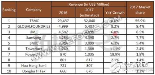
Figure 1: The top ten foundry makers by revenue (Samsung, Power's data are estimates).
More data
WSTS recently predicted that the semiconductor market in 2017 will reach US$409 billion, an increase of 20.6% over 2016. The increase in revenue is due to the increase in the average selling price of DRAM. And strong demand for analog, flash, and logic.
The WSTS expects the IC industry market will reach US$437 billion in 2018, an increase of 7% from 2017. According to the statistics of VLSI Research, the total IC is expected to increase by 7.1% in 2018, compared with 12.8% in 2017.
For many years, the IC industry has been constantly changing around Moore's Law (the transistor density has doubled every 18 months). According to this law, chip manufacturers will introduce a new process every 18 months, ostensibly to reduce the cost of the transistor.
At present, Moore's Law is still feasible, but it is experiencing new developments. Every time a new node is experienced, the cost and complexity of the process are rapidly increasing. Therefore, a fully expanded node rhythm has been extended from 18 months to 2.5 years or longer. In addition, fewer OEM customers can afford the ability to transition to advanced nodes. According to Gartner, the chip design cost for a 16nm/14nm chip is about 80 million dollars, and the chip design cost for the 28nm chip is 30 million dollars. In contrast, designing a 7nm chip costs US$271 million.
As always, mobile phones are still the largest market for the chip industry. According to IC Insights, mobile IC sales account for 25% of the IC market's total revenue and are expected to reach US$97.3 billion in 2018, an increase of 8% over 2017. The agency also believes that PC-related chips are the second-largest IC market and are expected to increase by 5% in 2018 to reach US$72.6 billion.
The growth rate in other markets is even more alarming. For example, automotive IC sales are expected to increase by 16% in 2018 to 32.4 billion U.S. dollars; by 2018, IC sales related to the Internet of Things will increase by 16% to approximately 16.8 billion U.S. dollars.

Figure 2: Market Growth in the IC Sector (in billions of dollars)
“More and more customers are redefining their product portfolio to adapt to the Internet of Things and the automotive market,†said Walter Ng, UMC’s US sales vice president. “In the automotive field, information entertainment, data security, and advanced operating functions are Progress, is increasing the demand for MCUs, which integrates embedded non-volatile memory, RF components and MEMS sensors.
WalterNg also said: "In the Internet of Things, we have seen many different types of devices, but the main focus seems to be integrated ICs that integrate MCUs with multiprotocol communications, including Wi-Fi, Bluetooth and even Zigbee. We also look The company has great interest in home automation."
Taking into account these growth drivers, OEMs must develop more different processes to meet the growing needs of their customers. Gary Patton, chief technology officer of GlobalFoundries, said: "A technology platform that can meet everything from high-end IBMz systems (mainframes) to battery-powered IoT devices is clearly impractical."
To meet these requirements, fabs must increase their capital expenditures and R&D expenditures annually. However, only a few fabs have the resources to develop multiple technologies. Smaller companies are certainly feasible, but they must be more specific to the market.
In addition to R&D capital expenditures, there are some challenges that wafer foundries need to face:
Economic and political issues may affect the electronics industry.
Poor demand and inventory problems tend to occur in the first quarter, which may persist in the subsequent quarters.
The integrated circuit business is undergoing a wave of mergers and acquisitions. The result of the integration is a reduction in the customer base of OEMs.
The availability of silicon is worrying. After years of oversupply, silicon suppliers saw new demand. However, the suppliers did not invest in new factories and many companies have already raised prices.
Packaging test supply chain is another issue for fabs. The rise in demand for chips has led to a shortage of manufacturing capabilities, various package types, and even some devices.
10nm/7nm, 22nm Process Technology Migration
By 2018, Intel is expected to increase its input by 10 nanometers. In addition, GlobalFoundries, Samsung and TSMC will begin shipping their respective 7nm finFET process products. Samsung also announced various half-node products.
The node name is very confusing. In short, Intel's 10nm technology is roughly equivalent to the 7nm node of other fabs.
In any case, node migration is challenging. For example, some chip makers spend longer than expected migrating from planar nodes to 16 nm/14 nm. In the 16nm/14nm process, many vendors are turning to the next generation of transistor types called FinFETs. In FinFETs, the control of the current is achieved through the gates on the three sides of the fins.

Figure 3: FinFET and Plane
In general, FinFETs solve short-channel effects and other scaling issues, but the technology is more difficult and costly to manufacture.
For example: Intel should have released a 10-nm FinFET process in the second half of 2017, but recent progress has slowed. Abhinav Davuluri, analyst at Morningstar, an investment banking firm, said in a recent interview: “The Intel 10nm FinFET process looks like it was postponed until the first half of 18 years.†This may have been a series of problems. However, their time to solve the 14-nm process problem is essentially doubled in the 10nm process. Because now you are doing self-aligned four-axis mode, not dual mode. It requires more steps and better functional dimensions. Obviously these two issues are contradictory. â€
From a time point of view, GlobalFoundries, Samsung and TSMC will face similar problems at 7nm. Gartner analyst Samuel Wang said: "The three foundries seem to be making good progress."
Samuel Wang expects that there will be a big increase in 7nm process in 2018, but in the short term, it cannot compete with 10nm at all. It is estimated that in 2017, 10nm will generate a business valued at 5 billion U.S. dollars. In contrast, by 2018, 7nm sales are expected to increase from $2.5 billion to $3 billion.
So how will 7nm evolve over time? "This is a gradual process," said Patton of GlobalFoundries. "Some customers are more actively planning to the next node. Others will follow up slowly."
According to Patton, 7nm will be a longevity node. FinFETs will have many extensions and have a lot of room for expansion.
TSMC said that the 7nm node may achieve the same achievements as 28nm. “The initial applications of 7nm were high-end application processors and high-performance computing. We expect there will be more than 50 tapeouts by the end of 2018,†said CCWei, co-CEO and president of TSMC in a recent teleconference.
However, not all foundry customers are world leaders. Although many companies are developing new chips, they are exploring the idea of ​​migrating to 16nm/14nm and beyond. However, many companies stay above the 28-nm node because they cannot afford the high IC design costs of advanced nodes.
To fill the market gap, GlobalFoundries, Intel, TSMC and UMC are developing a new 22nm process. 22nm is faster than 28nm and chip development costs are lower than 16nm/14nm.
However, not all 22nm technologies are the same. For example, GlobalFoundries is preparing 22nm FD-SOI technology. TSMC and UMC are developing a 22nm high-capacity CMOS process. Intel, on the other hand, adopted a new low-power 22nm FinFET technology.
Since then, customers must weigh various options. "It depends on what space you are in," Patton of GlobalFoundries said: "If you focus on high performance and are trying to make large chips, then you will choose FinFET. If you expect the chip size is small, and the cost and power consumption reach Balance, then you can follow the FD-SOI path.
Large-capacity CMOS process is also an option, UMC is developing a 22nm process for RF, millimeter wave and other applications. "This process offers the best combination of performance and cost," said Raj Verma, vice president of UMC's expertise division.
In spite of this, many fab customers will continue to use 28nm in the future. Gartner's Wang said: "The 28nm technology provides the best combination of speed, power and cost, and it will continue to maintain good demand. The 28nm wafer foundry revenue can reach $10 billion annually."
So, will 22nm take off? "Yes, because 22 nm is an extension of 28 nm," said Wang. "It provides better performance and density."
8-inch wafer boom
In the past two years, due to the surge in demand for certain chips, the IC industry has a serious shortage of 8-inch wafer fabs.
In 2018, the 8-inch supply will remain tight, and the 12-inch supply is expected to follow a similar path. "The year 2018 will be the third year of tight supply for 8-inch technology," UMC’s Ng said. "With the 12-inch technology capabilities starting to follow, we see that the customer sourcing strategy is beginning to become more strategic."
In general, a typical 8-inch fab produces about 40,000 wafers per month, producing chips ranging from 6 microns to 65 nm. Ng said: "Traditional MCUs, power discretes, PMICs, fingerprint sensors, and display-driven chips are still larger than current needs."
All in all, the 8-inch demand will continue for some time, prompting chip makers to find new and creative ways to deal with capacity deflation. For example, chip manufacturers have moved some devices from 8 inches to 12 inches. 12-inch wafer fabs have been able to produce high-end chips.
Ng said: "12-inch technology is expected to move toward higher utilization. The traditional 12-inch process is mainly driven by applications such as power management, fingerprint sensors and display driver ICs, while the more mainstream 12-inch demand is driven by MCUs. Communication and storage application drivers."
On mature nodes, fabs can provide specialized processes such as analog, bipolar CMOS-DMOS (BCD), MEMS, mixed-signal, power management, and RF.
Today, due to the advent of 5G and cars, professional foundry business is revitalizing. Power electronics and wireless are still growth markets. Ng said: "UMC is in the growth phase of BCD power management applications, driven by new global energy sources, which will require more complete, safe and available power management solutions.
At the same time, the automotive market is still a small part of the overall foundry business, but this area is growing rapidly. Therefore, the foundry is competing to expand its business in the arena.
MarkGranger, vice president of GlobalFoundries Automotive, said: "In the past few years, we have begun to see a real turning point, you can start to see the semiconductor content in the vehicle began to grow. With the ADAS, these increases are particularly evident."
In general, the automotive field is divided into five main sections: Body, Connectivity, Convergence/Security, Infotainment and Powertrain.
Fabs have seen demand for chips in all areas. Some areas will grow faster. "In the field of electrification of automobiles, safety systems and electric trains, these fields are driving semiconductor development," said Marco Racanelli, Senior Vice President and General Manager, RF/High Performance Simulation at TowerJazz.
OEMs are also stepping up their advanced driver assistance systems (ADAS) and autopilot technologies. ADAS involves various safety functions in the car, such as automatic emergency braking and lane detection.
Luxury cars already contain many ADAS features. The goal now is to incorporate these security features into mid-range and entry-level models. This will be related to costs and will take some time to progress. In spite of this, the emergence of fully automatic driving still has to wait for several years or even decades.
In addition to automobiles, 5G is another potential big market for OEMs, equipment manufacturers and foundries. 5G is a follow-up product of the current 4G and LTE wireless standards. It will make the data transfer rate exceed 10Gbps, or 100 times the throughput of LTE.
If 5G takes off, the technology will drive the development of new chips for infrastructure and mobile phones. TowerJazz's Racanelli said: "Faster, more mobile data requirements are driving the urgent need for expansion of hyperscale data centers and cloud computing centers, and will create future opportunities for mobile 5G systems.
Racanelli said: "Data centers need more specialized semiconductors from power management to high-speed fiber front-ends. 5G systems will make RF front-ends more complex and require more RF-soi switches, filters and amplifiers. Finally, 5G also Including a 28GHz band, our customers and partners have already created 12Gb/s connections in advanced SiGe."
However, UMC’s Ng stated: “In the short term, there is still doubt as to how the infrastructure will evolve to support the 5G radio frequency of currently defined Wi-Fi and routers and smartphones below 6GHz. 5G infrastructure deployment needs It will take a long time for the general public."
Chinese market opportunities
The Chinese market is a huge opportunity for wafer manufacturers. SMIC and other Chinese foundries are continuing to expand. UMC, a foreign company, has established a new 12-inch wafer fab in China. GlobalFoundries, TowerJazz and TSMC are building new factories in China.
The foundry business will not only produce chips for multinational IC manufacturers, but will also provide chips for more and more domestic fabless design companies. According to TrendForce's statistics, in 2017 China's IC design industry revenue is expected to increase by 22%. According to the research company's data, by 2018, the growth rate is expected to remain at about 20%.
JereTeo, research director at TrendForce, said: "This growth will be attributed to the IoT market, where AI and 5G solutions will also drive the expansion." Other opportunities will come from emerging applications such as biosensors and fingerprints for fingerprint and facial recognition. Photo and AMOLED. â€

Figure 4: Growth of China's IC design industry

Figure 5: China Semiconductor Fab Design Company ranked by revenue
Although the industry is closely watching the semiconductor industry in China, we should also pay attention to China's efforts in the application field. According to LungChu, president of SEMI China, China is pursuing the development of technologies such as 5G, Industry 4.0 and smart grid. In some areas, China is growing faster than the rest of the world.
The method of wax loss originated in the Spring and Autumn Period. The bronze ban of the Spring and Autumn Period unearthed from the Chu Tomb no. 2 of Xiasi in Xichuan, Henan province is the earliest known wax loss casting. The four sides and sides of the bronze ban are decorated with carved moire pattern. There are 12 vertical carved animals around the bronze ban, and 10 vertical carved animal feet under the bronze ban. The carving patterns are complicated and changeable, and the shape is gorgeous and solemn, which reflects that the wax loss method has been relatively mature in the middle of spring and Autumn period. After the Warring States, Qin and Han dynasties, the wax loss method became more popular, especially during the Sui and Tang dynasties to the Ming and Qing dynasties, the wax loss method was mostly used in casting bronzes.
Investment Casting,Lost Wax Casting,Steel Investment Casting,Stainless Steel Investment Casting
Tianhui Machine Co.,Ltd , https://www.thcastings.com