Common on-chip filters have a design bandwidth of megahertz, while filters with tens of kilohertz bandwidth are mostly implemented with off-chip passive components. The reason is that the low-frequency filter has a large time constant and occupies a large amount of chip area in the chip.
The usual way to achieve huge time constants on-chip is to combine large resistors and small capacitors. Because large resistors can be implemented using switched capacitor technology. Previously, the filter implemented by switched capacitor technology has two obvious drawbacks: one is that the switched capacitor introduces a lot of noise in the signal path, which directly leads to the linearity of the filter; the second is that the clock frequency of the switched capacitor must be Subsequent ADC frequencies are strictly consistent, otherwise it will result in lost codes.
This article still uses switched capacitor technology, but not in the signal path, but put it in the control circuit. The resistor in the main path uses an R-MOS structure, and the resistance can be precisely adjusted by the control circuit. This not only utilizes the switched capacitor to accurately realize the function of the large resistor, but also eliminates the two defects mentioned above, so that the linearity of the continuous time filter can be achieved.
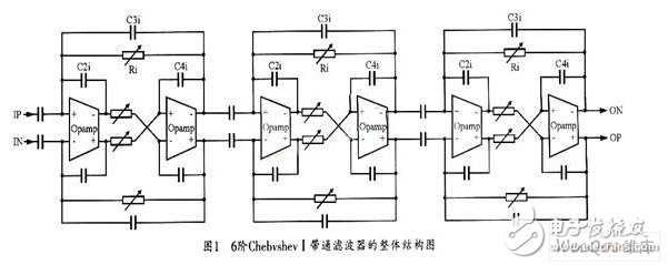
1 filter structure The overall structure of the filter is shown in Figure 1. In the picture, ![]() The overall structure has three levels, each of which is a second-order bandpass filter of High-Q Opamp-RC, which is cascaded to form a 6th-order Chebvshev I-type filter. The overall transfer function of the filter is as follows:
The overall structure has three levels, each of which is a second-order bandpass filter of High-Q Opamp-RC, which is cascaded to form a 6th-order Chebvshev I-type filter. The overall transfer function of the filter is as follows:

In order to reduce the complexity of the circuit. All the resistors in Figure 1 use the same resistance, so that the entire filter only needs one control.

Since the value of the resistor varies greatly with the PVT, in order to make the frequency response characteristic of the filter unaffected by the PVT variation, the resistance value is not required to vary with the PVT. To do this, it is necessary to discuss how to ensure that the resistance value does not change with the PVT change.
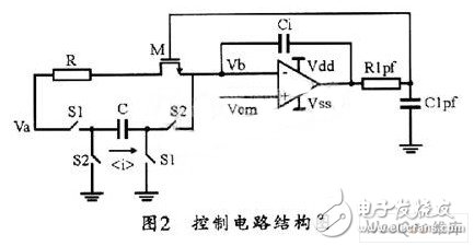
2 precision resistance processing The precision resistor is realized by the control circuit part, and its control circuit structure is shown in FIG. 2. The switches S1 and S2 can be respectively controlled by the two-phase non-overlapping clocks φ1 and φ2 to periodically charge and discharge the capacitors, thereby making the equivalent resistors ![]() The MOS tube M operates in the linear region and its resistance is as follows:
The MOS tube M operates in the linear region and its resistance is as follows:

The value of Ri can be obtained by RM and R. When Ri"Req, the integrator exhibits a positive integral characteristic, the output voltage of the op amp increases, VGS becomes larger, RM becomes smaller, and Ri becomes smaller.

In Figure 2, the role of R is to lower the voltage at the drain terminal of the MOS transistor, allowing the MOS transistor to operate in the linear region to increase the linearity of the resistor RM.
The resistor Ri in FIG. 1 is the same as the resistor Ri in FIG. 2, and they are all controlled by the control signal VCtrl. The time constant in Figure 1 is as follows:


Where T is the clock period, Ci is the integral capacitor, and C is the equivalent resistor capacitor. In order to improve the capacitance matching, C and Ci should use the same unit capacitance combination, so that equation (3) can be changed to:

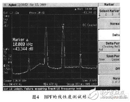
Figure 4 shows the linearity test results of the filter. The input is two in-band single-frequency signals with an interval of 10 kHz. The signal amplitude is 500 mVpp, and the output is detected by an oscilloscope. The linearity test results are 43 dB, which shows that this design has a high degree of linearity.

Since the time constant of the filter designed in this paper is only related to the frequency and capacitance ratio. Therefore, as long as the clock frequency is changed, the center frequency of the filter can be changed. In addition, using the method of this paper, it is also possible to make the filter inside the chip, so that with the switched capacitor technology, the area of ​​the chip only needs to increase by a small part. At present, the chip has been mass-produced under the SMIC 0.18μm process.
Insulated Terminals,Terminals,High-quality insulated terminals
Taixing Longyi Terminals Co.,Ltd. , https://www.longyiterminals.com