PCB (Printed Circuit Board), the Chinese name for printed circuit boards, also known as printed circuit boards, is an important electronic component, a support for electronic components, and a carrier for electrical connection of electronic components. Because it is made by electronic printing, it is called a "printing" circuit board.
After the electronic equipment adopts the printed board, due to the consistency of the same printed board, the manual wiring is avoided, and the electronic components can be automatically inserted or mounted, automatically soldered, and automatically detected to ensure the quality of the electronic equipment. Increase labor productivity, reduce costs, and facilitate maintenance.
Pcb features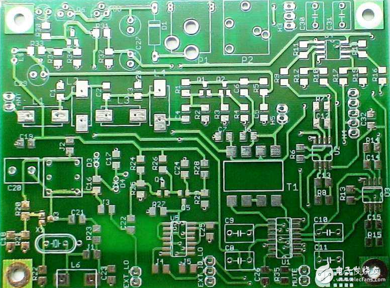
PCBs are becoming more widely used because they have many unique advantages, as outlined below.
1 can be high density. For decades, the high density of printed boards has grown with the integration of integrated circuits and advances in mounting technology.
2 High reliability. Through a series of inspections, tests and aging tests, the PCB can be reliably operated for a long period of time (usually 20 years).
3 Designability. For the various performances of PCB (electrical, physical, chemical, mechanical, etc.), the design of printed boards can be realized through design standardization and standardization, with short time and high efficiency.
4 Productivity. With modern management, it can standardize, scale (quantify), automate and other production, and ensure product quality consistency.
5 testability. Established relatively complete test methods, test standards, various test equipment and instruments to detect and identify PCB product qualification and service life.
6 assemblability. PCB products not only facilitate the standardized assembly of various components, but also can be automated, large-scale mass production. At the same time, the PCB and various component assembly components can be assembled to form larger components and systems up to the complete machine.
7 maintainability. Since PCB products and various component assembly components are produced in a standardized design and scale, these components are also standardized. Therefore, once the system fails, it can be replaced quickly, conveniently and flexibly, and the system can be quickly restored. Of course, you can say more about it. Such as miniaturization and weight reduction of the system, high-speed signal transmission, and the like.
The difference between PCB positive and negative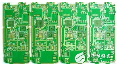
PCB positives and negatives are the opposite of the manufacturing process.
The effect of the PCB positive film: wherever the line is drawn, the copper of the printed board is retained, and the place where no line is drawn is removed. Such as the top layer, the bottom layer. . . The signal layer is a positive film.
The effect of the PCB negative film: Wherever the line is drawn, the copper of the printed board is removed, and the place where no line is drawn is preserved. Internal Planes layer (internal power/ground layer) (internal power layer) for arranging power and ground. The traces or other objects placed on these levels are copper-free areas, ie the working layer is negative.
What is the difference between PCB positive and negative output?
Negative film: Generally speaking, we are talking about the tenTIng process, and the liquid used is acid etching.
Negative film is because after the film is made, the desired line or copper surface is transparent, and the unnecessary part is black or brown. After exposure by the line process, the transparent part is chemically affected by the light of the dry film resist. Hardening, the subsequent development process will wash away the dry film without hardening, so only the dry film is etched away in the etching process to wash away part of the copper foil (the black or brown part of the film), while leaving the dry film is not Washing out the line that belongs to us (the transparent part of the film), after leaving the film, we leave the line we need. In this process, the film should be covered by the hole, and the exposure requirements and requirements for the film are slightly higher. Some, but the process of its manufacture is fast.
Positive film: Generally speaking, we are talking about the pattern process, and the liquid used is alkaline etching.
If the positive film is viewed from the negative film, the desired line or copper surface is black or brown, and the part is transparent. Similarly, after the line process exposure, the transparent part is chemically affected by the light of the dry film resist. Hardening, the next development process will wash away the dry film without hardening, followed by the process of tin-lead plating, plating the tin-lead on the copper surface washed by the dry film of the previous process (development), and then removing the film. Action (removal of dry film hardened by light), and in the next process etching, bite off the copper foil without tin-lead protection (the transparent part of the film) with alkaline syrup, and the rest is the line we want (negative film) Black or brown part).
What are the benefits of PCB positive film, and which are the main applications?Negative film is used to reduce the file size and reduce the amount of calculation. The place where there is copper is not displayed, and the place where there is no copper is displayed. This can significantly reduce the amount of data and computer display burden in the formation power layer. However, the current computer configuration is no longer a problem for this amount of work, I feel that it is not recommended to use negative film, it is easy to make mistakes. The pad is not designed to have a short circuit or something.
If the power supply is convenient, there are many methods. The positive film can also be easily divided by other methods. It is not necessary to use a negative film.
Pcb layout rules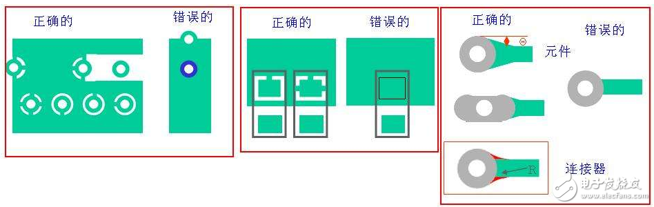
1. Under normal circumstances, all components should be placed on the same side of the board. Only when the top components are too dense, some devices with limited height and low heat can be placed, such as chip resistors, chip capacitors, and stickers. The chip IC is placed on the lower layer.
2. Under the premise of ensuring electrical performance, the components should be placed on the grid and arranged parallel or perpendicular to each other in order to be neat and beautiful. Under normal circumstances, the components are not allowed to overlap; the components are arranged in a compact manner, and the components should be on the entire layout. Uniform distribution, uniform density.
3. The minimum spacing between adjacent components of the board on the board should be less than 1MM.
4. The edge of the board is generally not less than 2MM. The optimal shape of the board is rectangular, and the aspect ratio is 3:2 or 4:3. When the board scale is larger than 200MM by 150MM, the board should be considered. Mechanical strength.
Pcb layout skillsIn the layout design of the PCB, the unit of the circuit board should be analyzed, and the layout design should be carried out according to its function. When all the components of the circuit are laid out, the following principles must be met:
1. Arrange the position of each functional circuit unit according to the flow of the circuit, so that the layout facilitates signal circulation and keeps the signal as consistent as possible.
2. Centering on the core components of each functional unit and surrounding it. Components should be evenly, integrally and compactly arranged on the PCB to minimize and shorten leads and connections between components.
3. For circuits operating at high frequencies, the distribution parameters between components should be considered. The general circuit should arrange the components in parallel as much as possible, so that it is not only beautiful, but also easy to install and easy to mass produce.
The location of special components is generally subject to the following principles when laying out:
1. Minimize the connection between high-frequency components and try to reduce their distribution parameters and mutual electromagnetic interference. Components that are susceptible to interference should not be too close to each other, and the input and output should be as far away as possible.
2 Some components or wires may have a higher potential difference, and their distance should be increased to avoid accidental short circuit caused by discharge. High-voltage components should be placed where they are not accessible by hand.
3. Components weighing more than 15G can be fixed by brackets and then soldered. Those components that are heavy and hot should not be placed on the circuit board and should be placed on the bottom plate of the main chassis, and the heat dissipation problem should be considered. The thermal components should be kept away from the heating components.
4. For the layout of adjustable components such as potentiometers, adjustable inductors, variable capacitors, microswitches, etc., the structural requirements of the whole wrench should be considered. Some switches that are often used should be allowed in the case of structure. Place it in a place where you can easily reach it. The layout of the components is balanced, dense and dense, and cannot be top-heavy.
Pcb wiring rules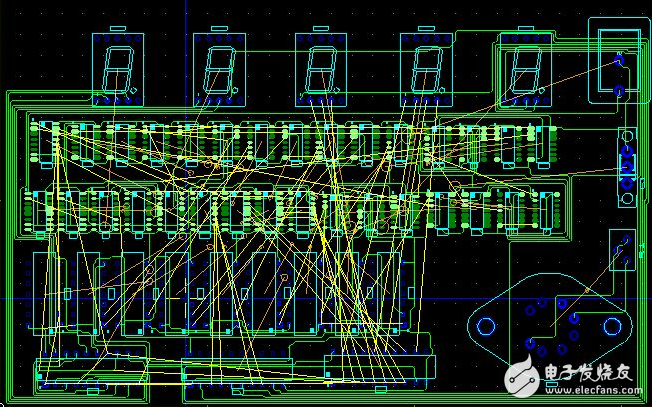
1. Draw wiring in the area where the wiring area is ≤1mm from the edge of the PCB board and within 1mm around the mounting hole.
2, the power cord should be as wide as possible, should not be lower than 18mil; signal line width should not be lower than 12mil; cpu input and output should not be lower than 10mil (or 8mil); line spacing is not less than 10mil;
3, the normal through hole is not less than 30mil;
4, double in-line: pad 60mil, aperture 40mil;
1/4W resistor: 51*55mil (0805 surface mount); pad 62 mil in diameter, 42 mil aperture; electrodeless capacitor: 51*55 mil (0805 surface mount); pad 50 mil in line, aperture 28 mil;
5. Note that the power and ground wires should be as radial as possible, and the signal wires should not have loopback traces.
Pcb design process specification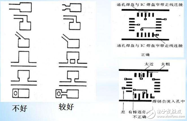
Rule 1: Select the correct grid - set and always use the grid spacing that matches the most components. Although multi-grid seems to have significant utility, engineers can avoid problems when setting up the interval and maximize the application of the board if they can think more at the beginning of the PCB layout design. Because many devices are available in a variety of package sizes, engineers should use products that are best suited for their design. In addition, polygons are critical for board copper placement. Multi-grid boards typically produce polygon fill deviations when performing copper-clad copper. Although not as standard as a single grid, they provide the board life beyond what is required. .
Rule 2: Keep the path shortest and most direct. This sounds simple, but it should be kept in mind at every stage, even if it means changing the board layout to optimize the wiring length. This is especially true for analog and high-speed digital circuits where system performance is always partially limited by impedance and parasitics.
Rule 3: Manage the distribution of power and ground lines as much as possible using the power plane. Power layer copper is a faster and simpler option for most PCB design software. By connecting a large number of wires in a common connection, the highest efficiency and minimum impedance or voltage drop current is guaranteed while providing a sufficient ground return path. If possible, run multiple power lines in the same area of ​​the board to verify that the ground plane covers most of the layer of a layer of the PCB, which facilitates the interaction between the lines running on adjacent layers.
Rule 4: Group the relevant components together with the required test points. For example, placing discrete components required for OpAmp op amps closer to the device allows bypass capacitors and resistors to collaborate with them, helping to optimize the wiring lengths mentioned in Rule 2, while also enabling test and fault detection. It's getting easier.
Rule 5: Repeat the copying of the required board on another, larger board for PCB imposition. Choosing the size that best suits the equipment used by the manufacturer helps to reduce prototyping and manufacturing costs. First make the board layout on the panel, contact the board manufacturer to get the preferred size specifications for each of their panels, then modify your design specifications and try to repeat your design multiple times within these panel sizes.
Rule 6: Integrate component values. As a designer, you will choose discrete components with high or low component values ​​but the same performance. By integrating within a smaller standard value, bills of material can be simplified and costs can be reduced. If you have a range of PCB products based on your preferred device values, it will be better for you to make the right inventory management decisions in the longer term.
Rule 7: Perform Design Rule Check (DRC) as much as possible. Although it takes only a short time to run the DRC function on the PCB software, in a more complex design environment, as long as you perform checks during the design process, you can save a lot of time, which is a good habit to keep. Every cabling decision is critical, and you can always remind you of the most important cabling by performing a DRC.
Rule 8: Flexible use of screen printing. Screen printing can be used to label a variety of useful information for future use by board manufacturers, service or test engineers, installers, or equipment commissioners. Not only the clear function and test point label, but also the direction of the components and connectors should be indicated as much as possible, even if these comments are printed on the lower surface of the component used on the board (after board assembly). Full application of screen printing technology on the lower surface of the board reduces duplication of effort and streamlines the production process.
Rule 9: Decoupling capacitors must be selected. Do not attempt to optimize your design by avoiding decoupling the power cord and depending on the limits in the component datasheet. Capacitors are inexpensive and rugged, so you can spend as much time as possible to assemble the capacitors, while following Rule 6, using standard values ​​to keep stocks tidy.
Rule 10: Generate PCB manufacturing parameters and verify them before submitting for production. While most board manufacturers are happy to download and verify it for you, it's best to export the Gerber file yourself and use the free viewer to check if it is as expected to avoid misunderstandings. By personally verifying, you will even find some negligent mistakes, and therefore avoid losing production by following the wrong parameters.
This scratch-resistant TPU Film protects your new AirTag from daily wear and tear. It can be easily glued to the back to keep the shiny silver in its original condition. In addition, the AirTag screen protector with "self-healing" function can automatically repair small scratches and bubbles within 24 hours. This means you can continuously enjoy the new look and appearance of AirTag without worrying about serious scratches and dents.
The Apple Airtag TPU Film can perfectly fit your AirTag skin. It is designed to provide the maximum coverage for your AirTag metal panels. Compatible with most AirTag shells. Leave extra space around the frame so that your shell can wrap the edges of the AirTag without interfering with the film.
The 0.14mm ultra-thin AirTag Screen Protector allows you to enjoy the maximum resolution while being thin enough to make the AirTag sensitive to the original signal response, ensuring that it will not affect any user experience. You won't even notice that the screen protector is there, so your Apple logo can still be displayed.
The AirTag Tracker Screen Protector is very easy to apply and is specially designed for your AirTag. Just clean your AirTag and install it on the surface to eliminate all bubbles and get the job done!
Apple Airtag Screen Protector, Apple Airtag Screen Protective Film, Apple Airtag TPU Film, AirTag Tracker Screen Protector, Skin Wrap
Shenzhen Jianjiantong Technology Co., Ltd. , https://www.mowang-dg.com