First, the problem from Hawking
It is said that Stephen Hawking once claimed that semiconductor manufacturers face two basic problems:
(1) limited speed of light
(2) The atomic nature of matter
The first problem is that in one CPU cycle, the electrical signal cannot be broadcast in all CPUs of the entire system. In other words, a CPU instruction writes to a memory address and will not be recognized by other CPUs immediately after the execution of this instruction. For example: CPU0 executes foo = 1 on the global variable foo. After CPU 0 executes the corresponding assembly code, other CPU cores still see the value before foo assignment. Readers who are new to the operating system need to pay attention to this.
The second problem is that we need at least one atom to store the binary bits. There is no way to store a word, a section of memory, or a complete register of contents in an atom... The end result is that hardware engineers have no way to reduce the chip area. As the CPU core increases, the burden of inter-core communication becomes even heavier.
Of course, as a theoretical physicist, Hawking's two questions are theoretical. It is very likely that semiconductor manufacturers are approaching these two limitations. Even so, there are some R&D reports that focus on how to circumvent these two basic limitations.
One way to circumvent the atomic nature of matter is a material called a "high-k insulator," which allows larger devices to mimic the electrical properties of ultra-small devices. There are some major production difficulties in this material, but it can finally push the frontier of research further. Another singular solution is to store multiple bits on a single electron, based on the fact that a single electron can exist simultaneously at multiple levels. However, this method remains to be seen to determine whether it can work stably in product-grade semiconductor devices.
There is also a solution called "quantum dots" that makes it possible to manufacture much smaller semiconductor devices, but the method is still in the research stage.
The first limitation is not easily bypassed, although quantum technology, and even string theory, theoretically allows communication speeds to exceed the speed of light. But this is only theoretical research, and it has not been applied in actual engineering.
Second, how slow is atomic operation?
The atomic operation here is specifically referred to in the Linux kernel, similar to the API of atomic_long_add_return. To put it simply, when an atomic operation is completed, make sure that all CPU cores have recognized modifications to the atomic variables, and that other CPU cores do not modify the variables during atomic operations. This necessarily requires that the corresponding electrical signal be broadcast between all CPUs. As shown below:
For normal variable operations (non-atomic operations), the electrical signal does not have to propagate between all CPU cores and pass back and forth:
One thing to forget: the Linux operating system can run on large systems with more than 1024 CPUs. In these large systems, it takes a "long" time to broadcast an electrical signal between all CPUs.
But how long is it?
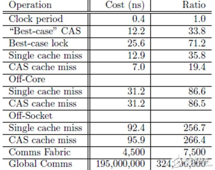
In the above table, the CPU cycle of a "CAS cache miss" is 266, is it long enough? And this test result is carried out in a relatively new multicore system with 4 core CPUs. In older systems, or in systems with more CPU cores, this is longer.
Third, variables can have multiple values
This is not a fantasy.
Assuming CPU 0 writes a value of 1 to the global variable foo, we naturally think that other CPUs will immediately recognize that foo has a value of 1. Even if there is some doubt, we may take a step back and think that at some later time, other "all" CPUs will "simultaneously" recognize that foo has a value of 1. There is no such strange phenomenon: at some point, CPU 1 recognizes that its value is 1, and CPU 2 recognizes that its value is zero. Unfortunately, it is time to say goodbye to this idea. Parallel computing is so magical and counterintuitive. If you can't understand this, there is no way to really understand the RCU.
To understand this, consider the following code snippet. It is executed in parallel by several CPUs. The first line sets the value of the shared variable to the current CPU ID, and the second line calls the gettb() function to initialize several values. This function reads the hardware time count, which is given by the SOC hardware and is available to all CPUs. Share between. Of course, this hardware count is mainly valid on the power architecture, and I often use it on the powerpce500 architecture. The loop of lines 3-8 records the length of time the variable is held on the current CPU.
1 state.variable = mycpu;
2 lasttb = oldtb = firsttb = gettb();
3 while (state.variable == mycpu) {
4 lasttb = oldtb;
5 oldtb = gettb();
6 if (lasttb - firsttb >1000)
7 break;
8 }
Before exiting the loop, firsttb will save a timestamp, which is the time of the assignment. Lasttb also holds a timestamp, which is the sampled value of the last value assigned to the shared variable. If the shared variable has changed before entering the loop, it is equal to firsttb.
This data was collected on a 1.5GHz POWER5 8 core system. Each core contains a pair of hardware threads. CPUs 1, 2, 3, and 4 record values, while CPU 0 controls the test. The timestamp counter period is 5.32 ns, which is sufficient for us to observe the cache status.
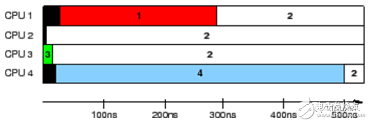
The results in the above figure show the time each CPU recognizes that the variable is held. Each horizontal bar indicates the time at which the CPU observed the variable, and the black area on the left indicates the time the corresponding CPU first counted. During the first 5 ns, only CPU 3 has the value of the variable. At the next 10 ns, CPUs 2 and 3 see inconsistent variable values, but then all agree that their value is "2". However, the CPU 1 considers its value to be "1" for the entire 300 ns, and the CPU 4 considers its value to be "4" for the entire 500 ns.
This is really an incredible test result. The same variable, even seen different values ​​on different CPUs! ! ! !
If you don't understand the hardware, you won't accept this incredible test result. Of course, if there is a master standing in front of you at this time, you can't dance with the rhythm of the master.
Fourth, why MESI
Please don't say: I don't know what MESI is?
Simply put, MESI is an in-memory cache coherency protocol.
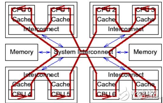
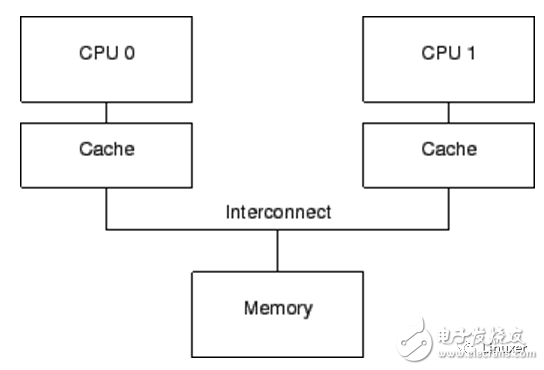
Modern CPUs are much faster than modern memory systems. The 2006 CPU can execute ten instructions per nanosecond. But it takes a lot of ten nanoseconds to get a piece of data out of physical memory. Their speed difference (more than two orders of magnitude) has led to the emergence of several megabytes of cache in modern CPUs. These caches are associated with the CPU, as shown below. Typically, the cache can be accessed in a few clock cycles. With the help of the CPU pipeline, we can assume that the cache can offset the impact of memory on CPU performance.
The data stream between the CPU cache and the memory is a fixed-length block called a "cache line", which is usually 2 N's in size. The range ranges from 16 to 256 bytes. When a particular piece of data is accessed by the CPU for the first time, it does not exist in the cache. This is called a "cache miss" (or more accurately called "startup cache miss" or "warmupcache miss"). "cache miss" means that when the CPU reads data from physical memory, it must wait (or "stalled") for hundreds of CPU cycles. However, after the data is loaded into the CPU cache, subsequent accesses will be found in the cache, so it can run at full speed.
After a period of time, the CPU's cache will be filled, and subsequent cache misses need to swap out the existing data in the cache to make room for the most recent access. This "cache miss" is called "capacitymiss" because it is caused by cache capacity limitations. However, even if the cache is not filled at this time, a large amount of cache may be swapped out due to a new data. This is because a large amount of cache is implemented by hardware hash tables. These hash tables have fixed-length hash buckets (or "sets", which the CPU designer calls), as shown in the following figure.
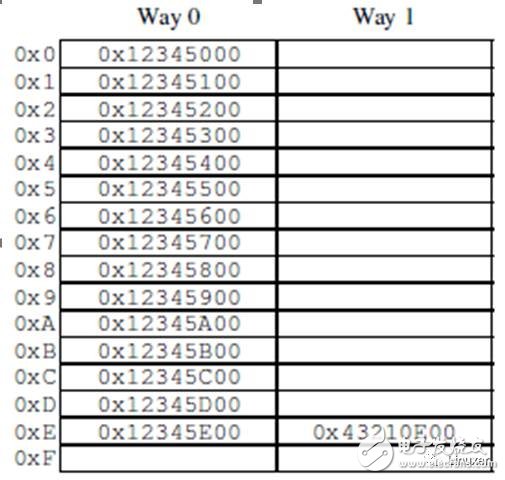
This cache has 16 "sets" and 2 "routes" for a total of 32 "cache lines". Each node contains a 256-byte "cache line", which is a 256-byte aligned block of memory. This cache line is slightly larger, but it makes hexadecimal operation easier. From a hardware perspective, this is a two-way set associative cache, similar to a software hash table with 16 buckets, with a hash chain of up to two elements per bucket. The size (32 cache lines in this case) and the connectivity (2 in this case) are called cache "geometry". Since the cache is implemented in hardware, the hash function is very simple: take 4 bits (the number of hash buckets) from the memory address as a hash key.
The situation in the figure may occur when the program code is at address 0x43210E00-0x43210EFF and the program accesses the address 0x12345000-0x12345EFF in sequence. Assuming the program is preparing to access address 0x12345F00, this address will be hashed to 0xF lines. Both lines of the line are empty, so the corresponding 256-byte cache line can be provided. If the program accesses the address 0x1233000, it will hash to the 0th line, and the corresponding 256-byte cache line can be placed on the 1st way. However, if the program accesses address 0x1233E00, it will hash to the 0xE line, and a cache line must be replaced to make room for the new line. If you subsequently access the replaced row, a "cache miss" will be generated, and such a cache miss is called "associativitymiss".
Furthermore, we only considered the case of reading data. What happens when I write? It is important to have all CPUs aware that the data has been modified before writing data to a particular CPU. Therefore, it must first be removed from other CPU caches, or "invalidated". Once the "make invalid" operation is completed, the CPU can safely modify the data item. If the data exists in the CPU cache but is read-only, this process is called "write miss". Once a particular CPU has caused other CPUs to complete the "make invalid" operation, the CPU can repeatedly rewrite (or read) the data.
Finally, if another CPU attempts to access the data item, it will cause a cache miss. At this time, because the first CPU invalidates the cache entry for writing, this is called "communication miss". This is usually because several CPUs use cache communication (for example, a lock for a mutex algorithm uses this data item to communicate between CPUs).
Obviously, all CPUs must be careful to maintain a consistent view of the data. These problems are prevented by the "cache coherency protocol", which is MESI.
Five, four states of MESI
MESI has four states: "modified", "exclusive", "shared", and "invalid". The protocol can apply these four states in a specified cache line. Therefore, the protocol maintains a two-bit status tag in each cache line, which is appended to the physical address and data of the cache line.
The cache line in the "modified" state is due to the recent memory storage of the corresponding CPU. And the corresponding memory ensures that it does not appear in the cache of other CPUs. Therefore, the cache line of the "modified" state can be considered "owned" by the CPU. Since the cache holds "latest" data, the cache is ultimately responsible for writing data back to memory, and should provide data for other caches, and must do so before caching other data.
The "exclusive" state is very similar to the "modified" state. The only difference is that the cache line has not been modified by the corresponding CPU. This also means that the data in the cache line and the data in the memory are up to date. However, since the CPU can store data to the line at any time regardless of other CPUs, the "exclusive" state can also be considered "owned" by the corresponding CPU. That is, since the value in physical memory is up to date, the line can be discarded directly without writing back to memory, and there is no need to notify other CPUs.
Cache lines in the "shared" state may have been copied to the cache of at least one other CPU so that data cannot be stored to the cache line without the permission of other CPUs. The same as the "exclusive" state, the value in the memory is the latest, so you can directly discard the value in the cache without writing back the value to the memory, and do not need to notify other CPUs.
The line in the "invalid" state is empty, in other words, it does not hold any valid data. When new data enters the cache, it is placed into a cache line that is in the "invalid" state. This method is better because replacing cached lines in other states will cause a lot of cache misses.
Since all CPUs must maintain a data consistency view in the cache line, the cache coherency protocol provides messages to identify the actions of cache lines in the system.
Sixth, MESI news
The MESI protocol requires communication between CPUs. If the CPU is on a single shared bus, only the following message is sufficient:
Read message: The "read" message contains the physical address of the cache line to be read.
Read Response Message: The "Read Response" message contains data for the earlier "read" message. This "read response" message may be provided by physical memory or by a cache of other CPUs. For example, if a cache is in the "modified" state, its cache must provide a "read response" message.
Invalid message: The "make invalid" message contains the physical address of the cache line to invalidate. Other caches must remove the corresponding data from their cache and respond to this message.
Invalid acknowledgment: A CPU that receives an "make invalid" message must respond to an "make invalid reply" message after removing the specified data.
Invalid read: The "read invalid" message contains the physical address to be read by the cache line. Also instruct other caches to remove data. Therefore, it contains both a "read" message and an "invalid" message. The "read invalid" message requires both a "read response" message and an "make invalid reply" message.
Write back: The "write back" message contains the address and data to be written back to physical memory. (and may "probe" the cache of other CPUs). This message allows the cache to swap out data in the "modified" state when necessary to make room.
Again, all of these messages require the propagation of electrical signals between CPUs, both of which face the two IT challenges that Hawking proposed.
Seven, MESI state transition
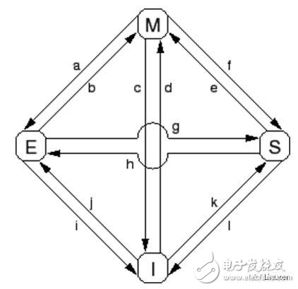
Transition (a): The cache line is written back to physical memory, but the CPU still keeps it in the cache and modifies it later. This conversion requires a "write back" message.
Transition (b): The CPU writes data to the cache line, which is currently in exclusive access. No need to send or receive any messages.
Transition (c): The CPU receives a "read invalid" message and the corresponding cache line has been modified. The CPU must invalidate the local copy and then respond to the "read response" and "make invalid reply" messages while sending data to the requesting CPU, indicating that its local copy is no longer valid.
Transition (d): The CPU performs an atomic read-modify-write operation with the corresponding data not in its cache. It sends a "read invalid" message and receives the data via a "read response" message. Once it receives a complete "make invalid response" response set, the CPU completes the conversion.
Transition (e): The CPU performs an atomic read-modify-write operation, and the corresponding data is read-only in the cache. It must send an "make invalid" message and wait for the "make invalid reply" response set to complete the conversion.
Transition (f): Some other CPUs read the cache line, the data is provided by the CPU, and the CPU contains a read-only copy. The reason for the read-only data may be because the data has been written back into memory. This conversion begins with the receipt of a "read" message, and eventually the CPU responds with a "read response" message.
Transition (g): Other CPUs read data and the data is provided from the cache or physical memory of the CPU. In either case, the CPU retains a read-only copy. The transaction begins with receiving a "read" message, and eventually the CPU responds with a "read response" message.
Transition (h): The current CPU will soon write some data to the cache line, so an "invalid" message is sent. The CPU does not complete the conversion until it receives all the "Invalid Reply" messages. Optionally, all other CPUs swap out the data of the cache line by "writing back" messages (possibly making room for other cache lines). Thus, the current CPU is the last CPU that cached this data.
Transition (i): Some other CPUs have performed an atomic read-modify-write operation, and the corresponding cache line is only held by the CPU. This CPU turns the cache line into an invalid state. This conversion begins with the receipt of a "read invalid" message, and eventually the CPU responds with a "read response" message and an "make invalid reply" message.
Transition (j): This CPU saves a data to the cache line, but the data is not yet in its cache line. Therefore, a "read invalid" message is sent. The transaction is not completed until it receives a "read response" message and all "make invalid responses" messages. Cache lines may transition to the "modify" state very quickly, which is done by Transition (b) after the storage is complete.
Transition (k): This CPU loads one data, but the data is not yet in the cache line. The CPU sends a "read" message and completes the conversion when it receives the corresponding "read response" message.
Transition (l): Other CPUs store a single row of data to the cache line, but the cache line is read-only (because other CPUs also hold the cache line). This conversion begins with the receipt of an "Invalid" message, and the current CPU eventually responds with an "Invalid Reply" message.
This article is not yet to be continued...
PGA Sockets Pin Grid Array Socket
A pin grid array, often abbreviated PGA, is a type of integrated circuit packaging. In a PGA, the package is square or rectangular, and the pins are arranged in a regular array on the underside of the package. The pins are commonly spaced 2.54 mm (0.1") apart, and may or may not cover the entire underside of the package.
PGAs are often mounted on printed circuit boards using the through hole method or inserted into a socket. PGAs allow for more pins per integrated circuit than older packages, such as dual in-line package (DIP).
PGA Sockets & Adapters
Low insertion force Pin Grid Array (PGA) Sockets and Adapters are available in a variety of RoHS Compliant insulators with hundreds of screw-machined terminal choices. Virtually any PGA footprint can be accommodated, including interstitial patterns.
PGA Sockets & Adapters Overview
Durable construction for virtually any application
Wide variety of materials, lengths, and sizes
Cost-effective method for replacing, repairing, or upgrading PGA devices
Unique options such as solder preform terminals eliminate the need for wave soldering in mixed SMT/Thru-hole applications
RoHS compliant insulators and screw-machined terminals are compatible with lead-free processing - select either Matte Tin/Gold (MG) or Gold/Gold (GG) plating
Antenk's Pin Grid Array (PGA) Sockets
Complex printed circuits are too valuable to risk direct soldering to expensive integrated circuits (ICs). Using a socket is the answer. The use of sockets offers advantages that prove cost effective and simplify board design.
Antenk's processor socket line is designed for use with Intel- and AMD-based microprocessor packages. Socket types include land grid array (LGA), micro pin grid array (mPGA), and PGA with low to zero insertion force. The mPGA and PGA sockets are designed for various microprocessor packages for notebook PCs, desktop PCs, and servers. For custom applications, the compression sockets can be configured to the specific application.
mPGA/PGA (ZIF)These sockets provide a zero insertion force (ZIF) PGA interface to the microprocessor PGA package and are attached to the PCB with surface-mount technology (SMT) soldering. PGA sockets are available in arrays up to 989 positions with single lever, screw driver, and hex wrench actuation methods.
PGA Sockets (LIF)
These sockets are primarily employed for microprocessor package test applications using through-hole solder attachment to the PCB design. The contacts are screw-machine outer sleeves with either stamped and formed or drawn inner contacts. Custom arrays are available in more than 1,000 positions.
Pin Grid Array (PGA) Sockets Type
mPGA
PGA

Eliminate hand-loading of pins, facilitate solder joint visibility, low profile component mounting or board mating.
PGA Sockets,mPGA Sockets,Integrated Circuits Socket,Pin Pga Sockets,Pga Socket Connector,PGA Adapters,Pin Grid Array Sockets,Processor Socket
ShenZhen Antenk Electronics Co,Ltd , https://www.antenkcon.com