Here to talk about the configuration circuit of xilinx spartan-3 series FPGA. Here is a list of the most common spartan-3 xc3s400 configuration circuits on the market. All spartan-3 FPGA configuration circuits are linked in the same way. Xc3s400 is a 400,000-gate FPGA. Although its ConfiguraTIonBitstream only has 1.699136Mbit, it still needs 2Mbit configuration chip XCF02S. I can't take it for granted that my design is simple and I use up to 1Mbit. Then I can choose XCF01S (1Mbit). This is not the case. Even if you just use xc3s400 to design a street light, then the data you download to ROM (XCF02S) is 1.699136Mbit, so the choice of FPGA configuration ROM should be small.
There are five types of configuration circuits: main string, slave string, master sum, slave, and JTAG. The first four are relative to the download to the PROM (string is different from the different configuration chip is the serial port and the time parallel port protocol and FPGA communication), only JTAG is relative to debugging is to download the configuration to the FPGA RAM (lost after power down). Compared with CPLD, CPLD is based on ROM type, which is to download data to CPLD and not lose it after power failure. The FPGA is based on RAM. If there is no external ROM to store the configuration data, then the data will be lost after power failure. Therefore, FPGAs need to have external configuration chips (of course, there are also FLASH-based FPGAs). Then we will look at the connection of the FPGA configuration circuit in the main string mode.
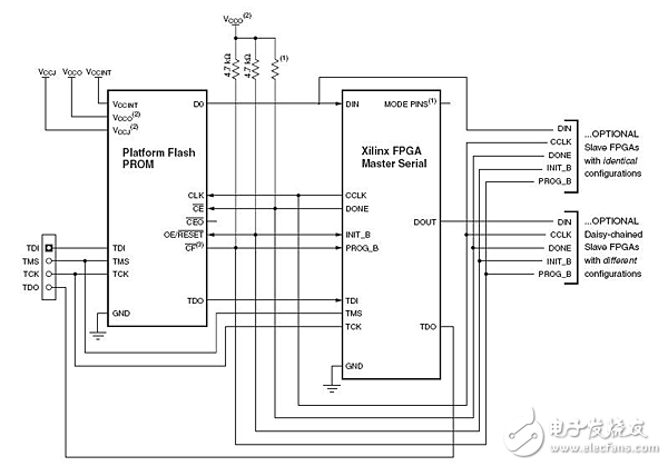
The official hardware connections are as follows:
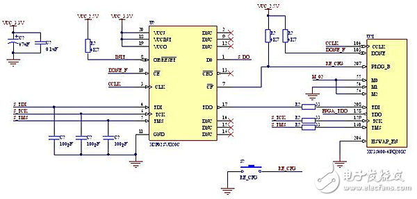
In order to increase the reliability of the configuration circuit, we usually add some anti-interference design (such as adding filter capacitors, matching resistors):
Look at the pins of the PROM chip first. According to the datasheet, the corresponding level is provided; the 3-pin CLK is connected to the CCLK of the FPGA, and the synchronization of the data communication is performed by the clock generated by the CCLK of the FPGA; since the chip is serially configured by the chip, there is only one data. The signal port DO is connected to the DIN port of the FPGA, and cooperates with the above clock signal to complete the serial data transmission. Whenever the rising edge of CLK latches the data, the address counter inside the PROM is automatically increased; there are also two control signals. When the line is INIT (OE/RESET connected to the PROM) and DONE (CE connected to the PROM), OE/RESET is to ensure that the address counter of the PROM is reset before each reconfiguration; regarding the CE pin, the official information is not very detailed. In my personal understanding, CE should be the abbreviation of chip enable. From the connection with the DONE pin of FPGA, it is not difficult to infer that when the FPGA is not configured, DONE=0, then the configuration chip PROM is in the chip select state, and once the configuration is completed. DONE=1, then the PROM is no longer strobed, and the datasheet also says that this pin can be directly grounded, that is, the chip is always selected, but this will make the DATA port have continuous data. The output of the number also causes unnecessary current consumption; the CEO pin is not connected here because it is used as the OE end signal connection of the next PROM in the configuration circuit of multiple PROMs; when the CF signal is connected to the PROG_B interface of the FPAG, Its role is to generate the start configuration signal, it is connected to a pull-up resistor, if PROG_B generates a low-level pulse, PROM will restart the configuration, so we will take a button to the ground on this line, if the button is pressed Then the PROM will be enabled to reconfigure the FPGA; there are also several signal interfaces TDI, TCK, TMS, TDO which are signals connected between the PROM and the PC. The PC downloads the data to the PROM through these circuits.
When talking about the signal interface of the PROM, the configuration pins of the FPGA are mentioned. Here are some more inductive explanations. The FPGA has 7 dedicated configuration pins and 4 dedicated JTAG pins (TDI, TCK, TMS, TDO). These pins are exclusively powered by VCCAUX (this series of FPGAs are usually connected to VCCAUX=2.5V). The M0, M1, and M2 pins of the FPGA are used for configuration mode selection. In the main string mode of the circuit, {M0, M1, M2} = 000, if the JTAG download mode {M0, M1, M2} = 101. The HSWAP_EN pin grounding not mentioned above is used to set the other idle pins to be pulled up when the FPAG is in the configuration state, and if the pin is connected to the high level, the FPAG is in the configured state and other idle pins. Floating. Therefore, in order to reduce the interference of the FPGA configuration process, this pin is generally grounded.
PCB Connectors: Backplane, Wire-to-Board, Board-to-Board Connectors
These types of connector systems are mounted or processed to a printed circuit board (PCB). There are a variety of PCB connectors and accessories best designed for specific uses. To name some, they include:Din41612 Connector,Board To Board Connectors,battery holders Clips Contacts,Future Bus Connectors,PLCC Connectors.
Din41612 Connector

Board To Board Connectors

Battery Holders Clips Contacts

Future Bus Connectors

PLCC Connectors

1.ANTENK manufactures a wide range of application specific board stacking PCB connectors which were designed and built to specific customer requirements. Our experienced staff has developed custom products in a variety of contact styles, pitches and stacking heights. Our designs range from new concepts to duplicating existing market products identically or with improvements. Many desigsn are produced using automated manufacturing processes to increase reliability and provide significant cost savings.
2.Our products are widely used in electronic equipments,such as monitors ,electronic instruments,computer motherboards,program-controlled switchboards,LED,digital cameras,MP4 players,a variety of removable storage disks,cordless telephones,walkie-talkies,mobile phones,digital home appliances and electronic toys,high-speed train,aviation,communication station,Military and so on
What is a PCB Connector?
Printed Circuit Board connectors are connection systems mounted on PCBs. Typically PCB Connectors are used to transfer signals or power from one PCB to another, or to or from the PCB from another source in the equipment build. They provide an easy method of Design for Manufacture, as the PCBs are not hard-wired to each other and can be assembled later in a production process.
PCB Connector orientations
The term PCB Connector refers to a basic multipin connection system, typically in a rectangular layout. A mating pair of PCB Connectors will either be for board-to-board or cable-to-board (wire-to-board). The board-to-board layouts can give a range of PCB connection orientations, all based on 90 degree increments:
Parallel or mezzanine – both connectors are vertical orientation;
90 Degree, Right Angle, Motherboard to Daughterboard – one connector is vertical, one horizontal;
180 Degree, Coplanar, Edge-to-Edge – both connectors are horizontal orientation.
Other names for PCB Connectors
PCB Connectors can be known as PCB Interconnect product. Specific terms are also used for the two sides of the connection. Male PCB Connectors are often referred to as Pin Headers, as they are simply rows of pins. Female PCB Connectors can be called Sockets, Receptacles, or even (somewhat confusingly) Header Receptacles.
Din41612 Connector,Board To Board Connectors,Battery Holders Clips Contacts,Future Bus Connectors,PLCC Connectors
ShenZhen Antenk Electronics Co,Ltd , https://www.antenkconn.com