According to Matsushita Electric Works, the lamp system that meets the JEL801:2010 specifications, the current goal is to meet the "LED" requirements of the fluorescent system that has entered the replacement period. This straight tube LED system reduces power consumption by approximately 42% compared to fluorescent systems. However, to meet the needs of the replacement, it is estimated that not only low power consumption, but also the performance of lighting from under the lamp to the wall is not inferior. At the time of product delivery, Panasonic disclosed development points for achieving good lighting performance.

New and old lighting fixtures are lit at the same time. Fluorescent light on the left and LED light on the right
Decentralized configuration of LED chips Â
The original straight tube type LED lamp always has many problems such as a plurality of LED light-emitting points being granular, light glare, color spots and chromatic aberrations, and light rays directed to the side direction (wall surface, etc.) are weak and cannot illuminate the entire room. This is also the reason why the user feels uncomfortable when replacing the fluorescent lamp with the LED lamp.
In order to solve these problems together, a long strip LED unit was used this time. On the ceramic substrate, a blue LED chip was mounted equidistantly upward and coated with a silicone resin mixed with a phosphor (Fig. 2). Light emitted from the surface and side directions of the blue LED chip causes the phosphor to emit light, thereby causing the entire LED unit to emit light. The use of a diffusion film between the glass tubes eliminates the graininess of the light-emitting points. The light loss caused by the diffusion film is only 2%.
Previously, because the packages of multiple LED chips were juxtaposed, there was no light-emitting between the packages. In addition, coating with a resin tube having a light diffusing function also caused a light loss of 10%.
Although the number of blue LED chips is not disclosed, a plurality of small-sized chips having a common shape are mounted 1) . The glare of the LED chip is finely dispersed, making the glare less dazzling. According to Matsushita Lighting Co., Ltd., which is responsible for the development of LED units, LED modules with multiple small chips mounted and packaged like this have been used in the development of LED bulbs .
Note 1) The general-purpose small blue LED chip has a single-sided size of 200μm to 300μm.


Thick Copper PCB are used extensively in power electronic devices and power supply systems. A growing trend in the PCB industry, this unique type of Heavy Copper PCB features a finished copper weight of more than 4oz (140μm), compared to the 1oz (35μm) or 2oz (0μm) copper weight generally found in those with a Standard PCB copper thickness.
The additional copper PCB thickness enables the board to conduct a higher current, achieve good thermal distribution and implement complex switches in a limited space. Other advantages include increased mechanical strength at connector sites, the ability to create a smaller product size by incorporating multiple weights on the same layer of circuitry and the ability to use exotic materials to their maximum capacity with minimal risk of circuit failure.
PCB Manufacture Capabilities
|
Features |
Capabilities |
|
Layers |
1-36 layers |
|
Material |
FR-4, Aluminum, Copper, Polyimide, high frequency (Rogers, PTEE, PI), etc. |
|
PCB Type |
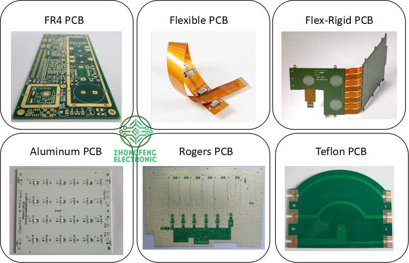
FR-4 Standard PCB, Aluminum PCB , Copper-based PCB, HDI PCB , Rigid-Flex PCB, Flex PCB, Thick copper PCB and Rogers PCB, etc. |
|
Board Thickness |
0.1mm-6.0mm |
|
Copper Thickness |
1/2oz-6oz(18um-210um) |
|
Biggest Board size |
600mm*1200mm |
|
Min Tracing/Spacing |
0.075mm/0.075mm (3mil/3mil) |
|
Min drilling Hole diameter |
0.15mm(6mil), 0.1mm(4mil)-laser drill |
|
Solder Mask |
Green, Black, White, Red, Yellow, Blue and Purple, etc. |
|
Silkscreen color |
White, Blue, Black, Red, Yellow |
|
Surface finish |
HASL Lead free, Immersion Gold (ENIG), Immersion Tin, Immersion Silver, OSP, Carbon oil, etc. |
|
Special Techniques |
Impedance Control, Gold Fingers, Blind/Buried vias, Peelable solder mask, Half holes, Via-in-Pad and Countersink hole, etc. |
PCB Products Show

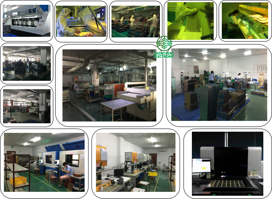
PCB Factory Show

Thick Copper PCB
Thick Copper PCB,Thick Copper PCB Board,Copper Thickness Tester PCB,Quality Thick Copper PCB
ZhongFeng Electronic Technology Co., Limited , http://www.dopcba.com