In today's world, designers seem to be constantly pursuing higher efficiency. We want higher power output with lower power input! Higher system efficiency requires team effort, including (but not limited to) higher performance gate drivers, controllers and new wide bandgap technology.
In particular, high current gate drivers can help improve overall system efficiency by reducing switching losses. Switching losses occur when the FET switch is turned on or off. In order to turn on the FET, the charge from the gate capacitance must exceed the threshold voltage. The drive current of the gate driver contributes to the charging of the gate capacitance. The higher the drive current capability, the faster the charge and discharge speed of the capacitor. The ability to pull a large amount of charge can reduce power loss and distortion. (Conduction loss is another FET switching loss. The conduction loss depends on the internal resistance or the RDS(on) value of the FET, where the FET dissipates power as the current passes.)
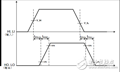
In other words, the goal is to reduce the switching transition time in the system that requires high frequency power conversion. Gate driver specifications that highlight this type of performance are rise and fall times. See Figure 1.
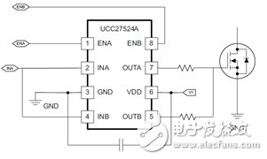
If you want to go further, gate driver characteristics such as delay matching can effectively double the drive current capability. Delay matching refers to the matching of the internal propagation delay between two channels, which can be achieved by parallel output of a dual-channel gate driver or by bundling two channels together. For example, TI's UCC27524A has an extremely accurate 1ns (typical) delay match that boosts drive current from 5A to 10A.
Figure 2 shows an example of the A channel B channel of the UCC27524A combined in a single driver. The INA and INB inputs, as well as OUTA and OUTB, are in series. The parallel combination is controlled by a signal.
One of the results of the increase in system efficiency is the increase in power density. In applications such as power factor correction (PFC) and synchronous rectifier blocks, DC/DC modules, and solar inverters for isolated power supplies, designers are constrained to achieve the same amount of output power in the same size (or smaller). Therefore, the demand for higher power density has become a trend.
TI's portfolio includes gate drivers with high current, fast rise and fall times and delay matching. See Table 1.
Start designing your high-efficiency system now! For more information, see www.TI.com/gate drivers.
Additional Information · The following TI designs show high current gate drivers in high efficiency systems:
· “High efficiency 400W AC/DC power supply reference design.â€
· “High efficiency 410W AC/DC power supply reference design.â€
In particular, high current gate drivers can help improve overall system efficiency by reducing switching losses. Switching losses occur when the FET switch is turned on or off. In order to turn on the FET, the charge from the gate capacitance must exceed the threshold voltage. The drive current of the gate driver contributes to the charging of the gate capacitance. The higher the drive current capability, the faster the charge and discharge speed of the capacitor. The ability to pull a large amount of charge can reduce power loss and distortion. (Conduction loss is another FET switching loss. The conduction loss depends on the internal resistance or the RDS(on) value of the FET, where the FET dissipates power as the current passes.)
In other words, the goal is to reduce the switching transition time in the system that requires high frequency power conversion. Gate driver specifications that highlight this type of performance are rise and fall times. See Figure 1.
Figure 1: Typical rise and fall time plots
If you want to go further, gate driver characteristics such as delay matching can effectively double the drive current capability. Delay matching refers to the matching of the internal propagation delay between two channels, which can be achieved by parallel output of a dual-channel gate driver or by bundling two channels together. For example, TI's UCC27524A has an extremely accurate 1ns (typical) delay match that boosts drive current from 5A to 10A.
Figure 2 shows an example of the A channel B channel of the UCC27524A combined in a single driver. The INA and INB inputs, as well as OUTA and OUTB, are in series. The parallel combination is controlled by a signal.
Figure 2: Serial output UCC27524A to double the dual drive current capability
One of the results of the increase in system efficiency is the increase in power density. In applications such as power factor correction (PFC) and synchronous rectifier blocks, DC/DC modules, and solar inverters for isolated power supplies, designers are constrained to achieve the same amount of output power in the same size (or smaller). Therefore, the demand for higher power density has become a trend.
TI's portfolio includes gate drivers with high current, fast rise and fall times and delay matching. See Table 1.
| classification | equipment | description | Rise/lower time | Delay matching |
High current driver | UCC27714 | 4A, 600V high side and low side drivers | 15ns, 15ns | stand by |
| UCC27524A | 5A, high speed low side dual drive | 7ns, 6ns | stand by | |
| UCC27211A | 4A, 120V high side and low side drivers | 7.2ns, 5.5ns | stand by |
Table 1: High Current Gate Drivers
Start designing your high-efficiency system now! For more information, see www.TI.com/gate drivers.
Additional Information · The following TI designs show high current gate drivers in high efficiency systems:
· “High efficiency 400W AC/DC power supply reference design.â€
· “High efficiency 410W AC/DC power supply reference design.â€
Gas Generating Set,Stable Performance Gas Generator,Gas Generating Set,Continuous Running Generator
Shaoxing AnFu Energy Equipment Co.Ltd , https://www.sxanfu.com