Rechargeable lithium batteries are widely used in handheld electronic products and industrial control fields. They need to continuously charge lithium batteries during use. A convenient and reliable charging circuit can not only improve the battery life, but also ensure the safety during charging. . The charging method can be charged not only by the USB interface but also by the direct connection of the 5V power adapter with the USB interface through the USB interface, and the method of charging only through the power adapter is more convenient. The field of lithium battery use itself requires a power supply voltage of 3.3V or 5V. When a lithium battery is used in a 3.3V operating control circuit, it needs to be stepped down by chopping or other means to meet The demand for use; when using a control circuit powered at 5V or higher, it is necessary to process the 3.7V of the lithium battery through the DC boost circuit to meet the requirements of the control circuit. This paper completes a set of control circuit required power supply voltage of 5V, using DC Boost boost circuit design.
2, lithium battery charging circuitThe lithium battery charging circuit discussed in this paper mainly consists of CN3052, which is a charge controller capable of cross-flow/constant voltage charging of a single-cell lithium ion or lithium-polymer rechargeable battery. The device internally includes a power transistor. No external current-sense resistors and blocking diodes are required for the application; the chip is also compatible with the USB bus specification and is very suitable for portable applications; for thermal modulation circuits, when the power consumption of the device is relatively large or the ambient temperature is high, The chip temperature is controlled within a safe range; the modulated output voltage is 4.2V with an accuracy of 1%, and the charge current can be rounded through an external resistor. When the input voltage is powered down, CN3502 automatically enters the low-power sleep mode. In this mode, the power consumption of the chip is on the order of microwatts. At the same time, the charging chip also has the functions of low input voltage detection, automatic charging, chip enable input, battery temperature monitoring and status indication.
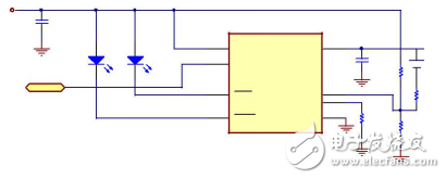
Figure 1CN3502 charging schematic
3. DC-DC conversion circuit 3.1, DC-DC conversion circuit classification and characteristicsThere are many types of DC-DC converters. According to whether the input/output circuits are isolated, they can be divided into two types: isolated DC-DC conversion and non-isolated DC-DC conversion. The isolated DC-DC converter has the advantages of wide switchable voltage range and good output waveform characteristics compared with non-isolated DC-DC; however, isolated DC-DC converters require transformers and other required elements. The device, so the space occupied in the circuit is large, the cost is high, etc., generally not suitable for smaller devices; the non-isolated DC-DC converter has less required components, light weight, small size and low cost. Excellent characteristics; the DC-DC converter involved in this paper is suitable for mobile phones, instrumentation and measurement and metering that can be carried around, so non-isolated DC-DC conversion is more suitable. For non-isolated DC-DC boost converter, it is divided into capacitive charge pump double voltage conversion and inductor DC-DC conversion. The design of charge pump double voltage conversion circuit is relatively simple. The components can be selected with appropriate capacitors. The interference is small, but it can only provide a limited range of voltage output. The voltage conversion of most charge pump ICs can only reach twice the input voltage, which means that the output voltage cannot be higher than twice the input voltage. The voltage output range is limited and the application is narrow; the inductive DC-DC converter has high output efficiency with respect to the charge pump, and the output voltage can be adjusted by the duty ratio as needed, and has a wide output voltage range, and the disadvantage is that In the circuit, the inductor needs to be charged and discharged, which increases the complexity of the circuit and also causes interference in the transaction. By comparing the advantages and disadvantages of various DC-DC conversions, this bit is intended to use inductive DC-DC conversion. This scheme has excellent characteristics in terms of cost, volume, efficiency and output voltage range.
3.2, the principle of inductive DC-DC converterInductive DC-DC conversion, the working principle is that the current flowing through the inductor cannot be abrupt, and the average voltage difference across the inductor is zero in one duty cycle. As shown in Figure 2 below, the DC-DC booster circuit works as shown in Figure 2. When the switch S is closed, energy flows from the input power source into the energy storage inductor L. At this time, the diode D is in the reverse bias state, and the ability to be stored in the filter capacitor C is released. To the load; when S is disconnected, because the current in the inductor L cannot be abrupt, the induced electromotive force generated by it prevents the current from decreasing, and the polarity of the induced electromotive force in L is left negative and positive, and the freewheeling diode D is in positive To the biased on state, the energy in the inductor is charged to the filter capacitor C through the freewheeling diode while powering the load.
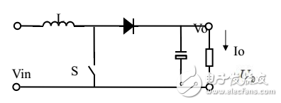
Figure 2 Inductive DC-DC boost schematic
During the closing of the switch S, the current flowing through the inductor L increases approximately linearly, and its value is: Equation 1 where is the minimum current value flowing through the storage inductor L. When the switch S is closed, the current flowing through the inductor L is: Equation 2 is available from Equations 1 and 2. The current flowing through the inductor L during the closing of the switch S is: Equation 3: When the switch S is open, the freewheeling diode Conduction, the voltage across the energy storage inductor is: Equation 4. The current flowing through the inductor L is: Equation 5 When the switch S is turned on, the current flowing through the inductor L is: Equation 6 The current change amount is: In the steady state, the increment of the current stored in the inductor L during the closing of the switch S is equal to the amount of decrease during the opening of the switch S, which is obtained by Equations 3 and 7: Equation 8: Equation 9.
Among them, it can be seen that changing the duty ratio can obtain the required voltage value. Since the duty ratio is always less than 1, the output voltage is always greater than the output voltage.
3.3, DC-DC conversion circuit designFigure 3 shows the schematic diagram of the DC-DC converter circuit designed in this paper. It can be seen from the DC-DC conversion schematic diagram shown in FIG. 3 that the conversion circuit is composed of a storage inductor L1, a switch controller MAX1771, a power MOS transistor IRF7403, a freewheeling diode IN5817, and a filter capacitor.
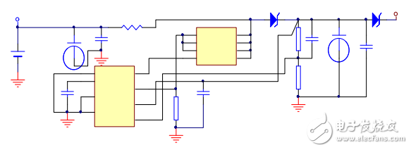
Figure 3 DC-DC conversion schematic
The MAX1771 is a switching power supply controller that uses a bipolar complementary metal oxide semiconductor process with a pre-fabricated output voltage of 12V and an adjustable output voltage configuration that combines PFM (Pulse Frequency Modulation) and PWM (Pulse Width) Excellent characteristics of modulation), high output efficiency and a wide range of output current. The pulse frequency modulation has a small quiescent current, and has high working efficiency under small load conditions, but the Wenbo wave is large; the pulse width modulation has high efficiency under large load conditions, and the cutting noise is small. The chip uses a new current-limited PFM control method to control the inductor charging current so that it does not exceed a certain current peak. This not only maintains the low quiescent current of the traditional PFM, but also has high working efficiency when working under a large load. At the same time, because the current peak of the inductor is limited, the peripheral circuit can obtain satisfactory information with fewer devices. The wave output voltage, which reduces the volume and reduces the cost. MAX1771 pin function introduction: 1) EXT is the N-channel power switch tube gate drive signal output pin; 2) V+ provides input power to the control chip, and also serves as the power supply detection output of the bootstrap mode; 3) FB is feedback detection The output terminal controls the output voltage through the detection circuit; 4) SHDN is the operation mode selection output pin, and the working sleep mode can be realized by controlling the input level of the pin; 5) REF is 1.5V reference voltage output, If not used, it can be grounded through 0.1uF capacitor; 6) AGND is the analog power ground; 7) GND is the power return ground; 8) CS pin is the current-limit output pin, and the overcurrent protection is realized by detecting the current of the power tube.
The MAX1771 peripheral circuit design, in order to achieve adjustable output voltage, needs to adjust the PFM frequency output by inputting the output voltage feedback to the FB pin of the MAX1771 and comparing the feedback voltage with the internal 1.5V reference voltage. As shown in FIG. 3, the feedback network is composed of a sum and a capacitor. The resistance and the resistance are selected to be between 10K and 500K, and the resistance value selected here is 100K. The resistance value obtained by the formula is 220K. For the choice of capacitance value, it is necessary to ensure the stability of the work and ensure the linear relationship. This value was selected here as 47 pF by experiment.
3.3.1, inductance determination
According to the operating waveform of the circuit, the inductor current includes a DC average and a ripple component. If the internal loss of the circuit is neglected, the output energy of the converter is equal to the input energy of the converter, that is, the waveform component of the inductor current is a triangular wave. During this period, the increment of the current is relative to the average current; The amount of current reduction is; when the circuit is operating in a steady state, the amount of current reduction is equal to the amount of current increase: in order to maintain the stability and reliability of the circuit operation, the peak current flowing through the inductor is generally not greater than its maximum average. 1.2 times the current while avoiding inductor saturation due to excessive current. The inductance value of the inductor can be determined by the following formula (Yang Xu. Switching Power Supply Design [M]. Beijing: Mechanical Industry Press, 2004.) where L is the critical inductance, the voltage output value, D is the duty cycle, T For the switching period, the current is the maximum output. Here it is 5.0V, D is 0.26, T is 20us, and the maximum output current is 1A. After calculation, the inductance of L is 7.12uH, and in this design, the inductance of L is 22uH/2A.
3.3.2, filter capacitor value determination
The output filter capacitor capacity is directly related to the request of the output voltage, and the output waveform voltage has a certain relationship with the duty cycle D. The expression of the output wobble voltage is: (Li Dingxuan, switch stable power supply design and application) From this formula, the capacitance value expression is: in this design, the input voltage is 3.7V, the duty ratio D is 0.26, MAX1771 The output frequency is set to 50KHz, and the waveform requirement for the output voltage is not more than 1%, so that the capacitance of the filter capacitor is 44uF.
3.3.3, the choice of switch tube
The maximum voltage that the switching tube VT is subjected to in the circuit is U0. Considering the influence of the input voltage fluctuation and the anti-peak spike voltage of the inductor, the maximum voltage of the switching tube should satisfy >1.1 & TImes; 1.2. Actually, when the switch tube is selected, the maximum allowable working voltage value of the tube should be left with sufficient room, generally (2~3) 1.1 & TImes; 1.2. The maximum allowable operating current of the switch tube is generally selected (2~3). The selection of the switch tube mainly considers that the switch tube drive circuit is simple, the switching frequency is high, and the on-resistance is small. This design selects the P-channel power FET IRF7404. The device has VDSM=20V and IDM=7A, which fully meets the design requirements.
4 Conclusion
According to the above principle and calculation design, input 3.7V, output 5V 5W step-up DC/DC circuit, the whole circuit is easy to debug, stable in operation, high in reliability, and the efficiency is more than 85%, especially low cost, which has been applied in practical equipment. . In addition, according to the specific circuit index requirements, the circuit can be flexibly controlled and changed to design other application circuits.
Pcb Board,Circuit Board,Pcb Electronics,Custom Pcb
Cixi Zhongyi Electronics Factory , https://www.cx-zhongyi.com