Hello, everyone, but also to the time of daily learning, a lot of people have recently asked me to learn whether FPGA is the choice of Altera's or xilinx's, so I said a lot of good-natured, the central idea is probably, learning FPGA must To learn FPGA design ideas and design principles, do not tangle on a single experimental platform or operating software, because you want to go higher and higher in this industry, the breadth and depth are to understand, early learning especially pay attention to Hands-on, choosing an operating platform and operating software is to allow you to do better, instead of allowing you to make a fuss on this software or experimental platform. If you don't understand the principle, you will also have nothing to change the environment. understand. Especially the upgrading and upgrading of the current technology company's products is still relatively fast, and it is the king to learn to master the most important knowledge points. Below, on my own contact, let's talk about the difference between FPGAs of Altera and Xilinx, welcome everyone to communicate together, three people, we must have our teacher, learn together, and make progress together.
For FPGAs of Altera and Xilinx, I think we can compare it with two aspects, basic logic resources and internal basic architecture.
From the perspective of the extensiveness of the development and use of the company, Xilinx is indeed larger, but other aspects, such as price, are relatively cheap compared to Altera. For the characteristics of both, Xilinx's short-term resources are very rich, so that when implemented, the success rate of the wiring is high, especially when the logic is relatively full. Altera's FPGA short-circuit resources are often not enough, often take LE to act as routing resources, which is why Altera's FPGA can be cheaper, less resources, of course, cheaper, but if you are a master, you can put his performance to play Very good. The other is about the block RAM, Xilinx's dual-port RAM is true, Altera's no dual-port RAM, if you want to achieve real dual-port RAM, you can only use two RAM to back-to-back to achieve, so your RAM resources are less Halfway, if your application's need for on-chip dual-port RAM is important, you won't be able to use Altera.
Let's talk about the basic logic resources and internal basic structure that I just mentioned.
1. Basic Logic Resources Basic Logic Resources I suggest that you can go and see the two chips to make a comparison. Today's limited time will not give you a detailed discussion. By comparison, you will find that what I said above is still a bit reasonable.
2. Internal basic architecture Since the introduction of the first FPGA by Xilinx in 1985, the use of FPGA has been used for nearly 30 years. At present, the FPGAs in the mainstream market are mainly two series of Xilinx and Altera. The following describes the basic structure of each of them. 
Xilinx's FPGA consists of the following cell structures: Configurable Logic Block (CLB), Clock Management Module (CMT), Memory (RAM/FIFO), Digital Signal Processing Module (DSP) and some dedicated modules. Take Virtex-5 as an example to briefly introduce the functions of each module.
1.CLB is the main resource of the FPGA that composes the design logic, and it is also the main object of the circuit design work. The following is a brief introduction to the internal and external structure of the CLB.
The logic of the FPGA is implemented by CLBs arranged in an array. Each CLB unit is connected to a switch array and controlled by it to implement logic, as shown in the following figure. 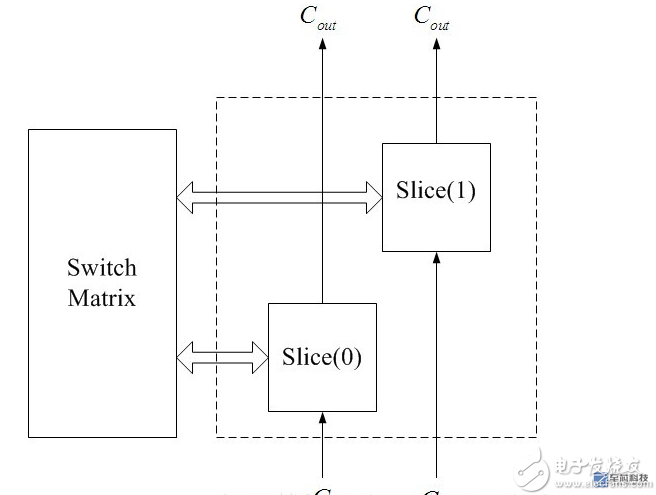
Each CLB contains two basic structures (Slices). Each basic structure contains 4 lookup tables (LUTs), 4 memory cells, Wide_function Multiplexer, and carry logic. This basic structure (Slice) is called SLICEL. In addition, some basic structures (Slice) also include the use of RAM to store data and the use of 32-bit register shift function, the basic structure to support these functions is called SLICEM.
2. Clock management module (CMT)
The clock management module (CMT) is used to generate high-quality clocks. Taking the Virtex-5 family of devices as an example, the CMT includes two digital clock management units (DCMs) and a phase-locked loop circuit (PLL).
3, memory (RAM / FIFO)
Modern Xilinx FPGAs have internal memory blocks. Take Virtex-5 as an example. Internally contains several blocks of RAM, each with 36KB, and the RAM size can be flexibly configured. The Virtex-5 RAM is a synchronous dual-port RAM and can be configured as a multi-rate FIFO memory, greatly improving the design flexibility.
4, digital signal processing module (DSP)
Most FPGA products provide DSP.
5. Other special modules In addition to the above modules, there are other special modules in modern Xilinx FPGA products, such as: Rocket IO gigabit transceivers, PCI Express endpoint modules, and tri-mode Ethernet MAC modules.
Altera's products typically include the following cell structures: logic array blocks (LABs), TriMatrix memory blocks (RAMs), digital signal processing blocks (DSPs), and phase-locked loop blocks (PLLs). The following uses the Startix II device as an example to illustrate the structure of Altera's products.
1, logic array module (LAB)
The main structure of the logic array module (LAB) is eight adaptive logic modules (ALM), and also includes some structures such as carry chain and control logic. The adaptive logic module (ALM) is the basic module of the Stratix II device. Its structure is shown in the figure below. 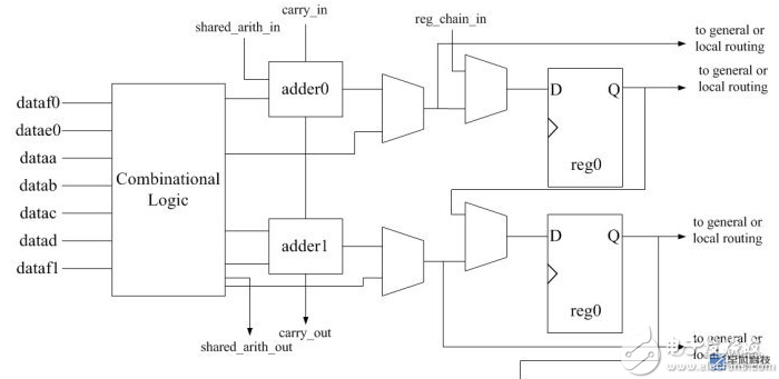
Each ALM contains two programmable registers, two dedicated full adders, a carry chain, a shared arithmetic chain, and a register chain. It should be noted that the Combinational Logic shown in the figure above contains two 4-input 4-lookup tables (LUTs) and four 3-input lookup tables.
2, memory module (RAM)
Stratix II devices have a TriMatrix memory structure that includes three sizes of embedded RAM blocks. TriMatrix memory includes 512-bit M512 blocks, 4Kb M4K blocks, and 512Kb M-RAM blocks, each of which can be configured to support various features.
3, digital signal processing module (DSP)
The DSP block structure is optimized for DSP functions that achieve multiple maximum performance and minimum logic resource utilization.
4, phase-locked loop (PLL)
Stratix II devices have up to 12 phase-locked loops (PLLs) and 48 independent system clocks that can serve as a central clock manager to meet system timing requirements.
It can be seen from the above that the structure of Xilinx and Altera's FPGAs is the most different from its logic unit: the Xilinx logic cells are basically composed of configurable logic modules (CLBs), while Altera's is LABs, but more deeply, CLBs and LABs. It is also composed of LUTs, triggers, and so on. The FPGA composition of the two companies has their own characteristics, which also determines the features of their FPGA products.
In general, Xilinx's unique configurable logic block (CLB)/Slice, and Altera's unique logic array module (LAB) can be understood as such.
Talk to you today, everyone!
USB Flash Drives Compatible iPhone/iOS/Apple/iPad/Android & PC 128GB [3-in-1] Lightning OTG Jump Drive 3.0 USB Memory Stick
1. 3-in-1 OTG USB flash drive for PC, iPhone, Android, Type C
2. USB 3.0 + Android + IOS interface;
3. Capacity from 16~128GB;
4. Auto-run Function is optional;
5. Bootable Function;
6. Built-in Password Protection;
7. High speed Performance;
8. Data transfer rate for Read is from 12MB/s to 25MB/s, for Write is 4MB/s to 14MB/s in Dual-channel mode;
9. Data transfer rate for Read is from 8MB/s to 15MB/s, for Write is 2MB/s to 8MB/s in Single-channel mode;
(The rate of performance depends on the different operation system available and various flash adopted).
10. Operation Systems supported: No driver needed in Windows ME, Windows 2000, Windows XP, Mac 9.x or later, Linux Kernel 2.4 or later. Only Windows 98 and Windows 98SE need the enclosed driver;
11. 10 years data retention;
12. More than 1,000,000 times data encryption;
13. Built-in Password Protection is optional (default setting: NO password function);
14. Auto-run Function is optional (default setting: NO auto-run function);
15. Bootable Function is optional (default setting: NO bootable function);
16. ReadyBoost Function under Windows Vista system is optional (default setting: NO readyboost function).
Iphone Ios Usb Flash Disk,Portable 2 In 1 , 3 in 1 Usb Pendrive,Otg Usb Flash Drives,Portable Otg Usb Flash Disk
MICROBITS TECHNOLOGY LIMITED , https://www.hkmicrobits.com