First, the radio frequency board laminated structure
In addition to considering the impedance of the RF signal line, the laminate structure of the RF PCB needs to take into account heat dissipation, current, device, EMC, structure, and skin effect. Usually we layer and stack the multilayer printed board. Follow the following basic principles:
A) Each layer of the RF PCB is covered with a large area, there is no power plane, and the upper and lower adjacent layers of the RF wiring layer should be the ground plane. Even in the case of digital-analog hybrid boards, there may be power planes in the digital section, but the RF area still has to meet the requirements for large-area paving at each floor.
B) For RF dual panels, the top layer is the signal layer and the bottom layer is the ground plane. The four-layer RF board has a signal layer on the top layer, ground planes on the second and fourth layers, and power and control lines on the third layer. In special cases, some RF signal lines can be taken in the third layer. More layers of RF boards, and so on.
C) For the RF backplane, both the upper and lower surface layers are ground. To reduce the impedance discontinuities caused by the vias and connectors, the second, third, fourth, and fifth layers take digital signals. The other stripline layers on the bottom surface are all RF signal layers. Similarly, the RF signal layer is two floors above and below the floor. Each floor should be covered with a large area.
D) For high-power, high-current RF boards, the RF main link should be placed on the top layer and connected with a wider microstrip line. This facilitates heat dissipation and reduces energy loss, reducing wire corrosion errors.
E) The digital part of the power plane should be close to the ground plane and arranged below the ground plane. In this way, the capacitance between the two metal plates can be used as the smoothing capacitor of the power supply, and the ground plane also shields the radiation current distributed on the power plane. The specific stacking method and plane division requirements can refer to the "20050818 Printed Circuit Board Design Specification - EMC Requirements" promulgated by the EDA Design Department. The latest standards on the Internet shall prevail.
Second, RF board wiring requirements
1. Corner
If the RF signal trace runs at a right angle, the effective line width at the corner will increase and the impedance will be discontinuous and cause reflection. Therefore, we must deal with the corners, mainly for the cutting angle and fillet two methods.
(1) Cut angles are suitable for smaller angles. As shown in the left figure, the cutting angle can be used up to 10 GHz.
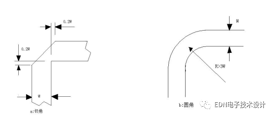
(2) The radius of the arc angle should be large enough. In general, it must be ensured that R>3W. As the right
2. Microstrip line layout
The top layer of the PCB goes through RF signals. The plane layer below the RF signal must be a complete ground plane, forming a microstrip line structure. To ensure the structural integrity of the microstrip line, the following requirements apply:
(1) The edges of the microstrip lines must have a width of at least 3W from the edge of the lower ground plane. In the 3W range, there must be no ungrounded vias.
(2) The distance from the microstrip line to the shielding wall should be maintained at 2W or more. (Note: W is line width).
(3) The uncoupled microstrip line in the same layer is to be processed in the copper ground of the package and ground vias are added on the copper ground. The spacing between the holes is less than λ/20 and they are evenly arranged. The edge of the copper foil should be smooth, flat, and burr-free. It is recommended that the edge of the copper cover be 1.5 W or more, or 3 H wide, from the edge of the microstrip line. H represents the thickness of the microstrip substrate media.
(4) Prohibit the RF signal traces from crossing the second floor ground plane gap.
3. Stripline wiring
The RF signal sometimes passes through the middle layer of the PCB. The common one is to go from the third layer. The second layer and the fourth layer must be the complete ground plane, that is, the eccentric stripline structure. Ensure that the structural integrity of the stripline requires:
(1) The edge of the stripline must have a width of at least 3W from the upper and lower plane edges, and in the 3W range, there must be no ungrounded vias.
(2) Do not allow the RF stripline to cross the upper and lower ground plane gaps.
(3) The strip line in the same layer is to be treated with a copper strip for the package and a ground via hole is added to the copper ground. The spacing between the holes is less than λ/20, and they are evenly arranged. The edge of the copper foil should be smooth, flat, and burr-free. It is recommended that the edge of the copper cover be greater than or equal to 1.5W width or 3H width from the edge of the stripline, and H represents the total thickness of the lower dielectric layer on the stripline.
(4) If the strip line is to transmit high power signals, in order to avoid the line width of 50 ohms being too thin, the copper skins of the two reference planes above and below the strip line area are usually hollowed out and the hollowing width is strip line. More than 5 times of the total thickness of the medium. If the line width still does not meet the requirements, the reference surface of the second layer adjacent to the top and bottom is hollowed out.
Fan commonly refers to a Solar DC Fan a mechanical fan fitted with a DC motor and solar panels that charge up the fan through solar energy:
- Fan (machine), a machine for producing airflow, often used for cooling.
- Hand fan, an implement held and waved by hand to move air.
Benefits
1.Inverter-friendly: compatible with existing inverter solutions
2.Extracool wind3.AC/DC Solar Compatible
4.600% Energy-saving
5.High money saving on Electric bills
Dc Ceiling Fan,12V Dc Fan,Dc Brushless Fan,Dc Table Fan
NANTONG RONGCHANG IMPORT&EXPORT CO.,LTD , https://www.ergsolarcn.com