The FTIR spectrometer (Fourier transform infrared spectroscopy) is a spectroscopic analyzer that analyzes the impurity concentration by Fourier transform using infrared spectroscopy, and can be used for gas and liquid analysis. Conventional FTIR spectrometers have the advantage of not requiring expensive image sensors, but because they require highly accurate optical spectrometers, equipment is often a relatively large and expensive benchtop instrument, which greatly limits the application of the device. "Smaller size" has become an important technical topic in the development of FTIR spectrometers.
When it comes to "small", people think of MEMS (Micro Electro Mechanical Systems) technology, which combines microelectronics technology with mechanical engineering to achieve a range of operations in the micrometer range. If this technology is integrated into the FTIR spectrometer, "desktop" and "handheld" should not be just a dream.
After many technical problems, Hamamatsu finally realized this concept and successfully developed Hamamatsu MEMS-FTIR products. It uses proprietary MEMS technology (the cutting-edge technology for 3D precision machining of semiconductor materials) to fabricate all optical splitting components on silicon wafers, ultimately achieving all the required optics on MEMS-FTIR drive components as large as fingertips. Function, based on this ultra-small MEMS-FTIR core drive original, Hamamatsu eventually developed the "handheld" MEMS-FTIR spectrometer.
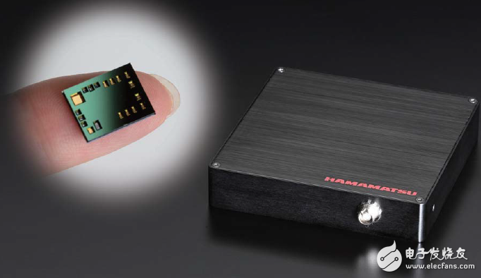
Hamamatsu MEMS-FTIR drive components and "handheld" MEMS-FTIR spectrometer C12606 (75x100x27mm)
Choice of MEMS technology
MEMS is a lightweight mechanical component of the smallest size achieved through a silicon wafer and semiconductor technology. A consistent process at the silicon wafer level enables mass production of MEMS. Based on silicon technology, it has obvious mechanical advantages in terms of high elasticity and high resistance. Integrated circuits make it easy to get multiple functions. In addition, the physical load caused by exposure can be ignored, so it is the best choice for MEMS drivers.
Hamamatsu MEMS-FTIR tightly integrates a Michelson interferometer and a movable mirror-controlled actuator in a silicon wafer-level package. An optical fiber that receives incident light is directly connected to the MEMS chip through passive alignment. This greatly reduces assembly costs. With DRIE (Deep Reactive Ion Etching), the relative position of each optical component of the MEMS-FTIR drive component is very precise, with a tolerance of no more than 1 μm, without any optical adjustment after assembly.
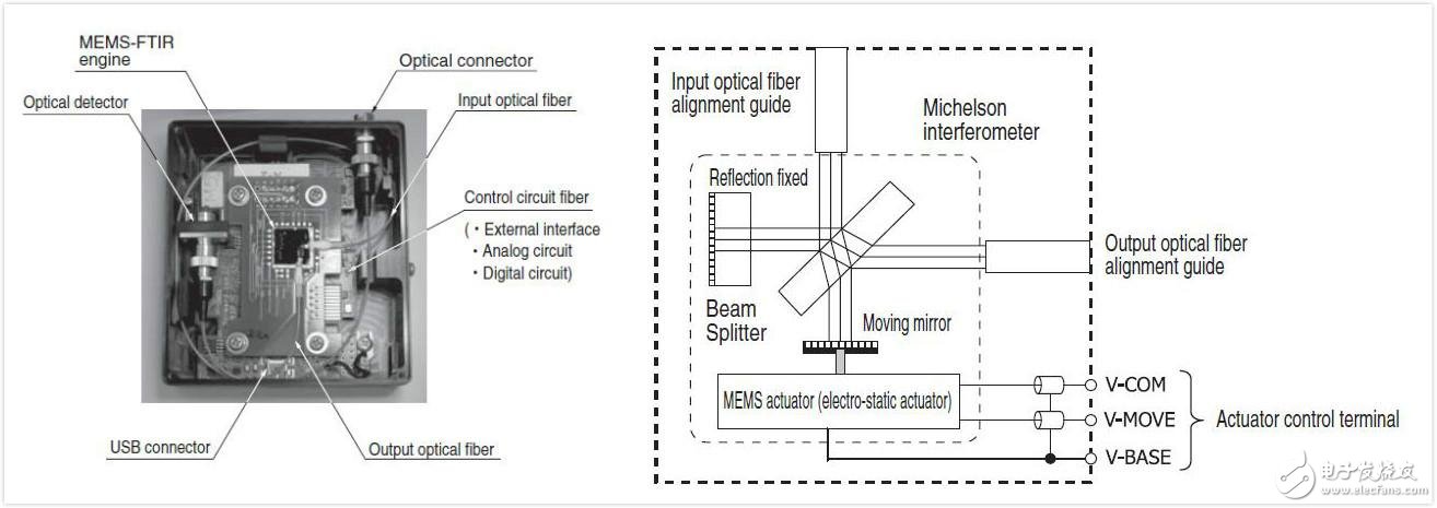
Hamamatsu MEMS-FTIR spectrometer C12606 and internal structure of the drive original
All optical components of the Michelson interferometer are formed on the walls of silicon. The beam splitter splits the incident beam by Fresnel reflection (reflection 30%; transmission 70%) by exploiting the large difference in refractive index between silicon and air. The moving mirror is placed on the electrostatic actuator and the fixed mirror surface, and each surface is formed by vapor deposition to form a metal layer, which forms a total reflection mirror surface with high reflectance (higher than 98%).
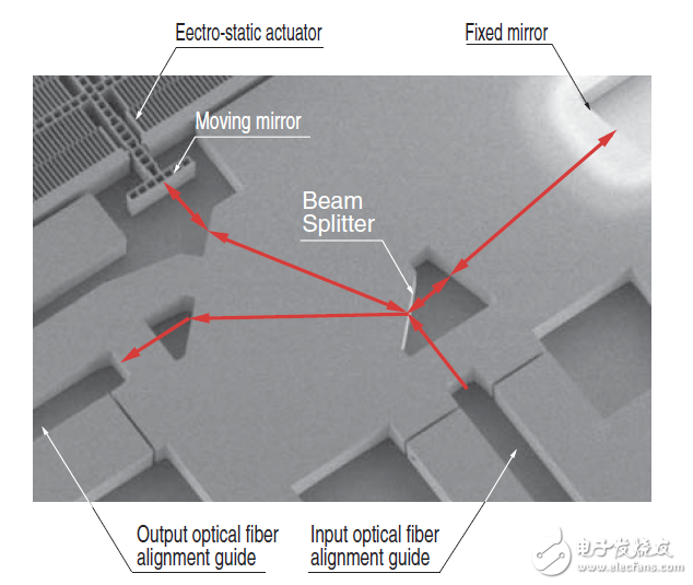
MIT image of Michelson interferometer
-------------------------------------------------- --------
This article is selected from the "Intelligent Hardware Special Issue" in April. More technical hot texts can be downloaded from the special issue page !

Double Sided Pcb,Double-Layer Circuit Boards,Double-Layer Pcb Circuit Board,Double Sided Circuit Board
Shenzheng Weifu Circuit Technology Co.Ld , https://www.wfcircuit.com