1 Introduction
Switching power supply has the characteristics of small size, light weight and high efficiency, and is widely used in communication, automatic control, household appliances, computers and other electronic equipment. However, its shortcoming is that the switching power supply operates under high frequency conditions, which generates very strong electromagnetic interference (EMI). The conduction and radiation will pollute the surrounding electromagnetic environment and affect the electronic equipment. This paper analyzes the circuit structure and device of the switching power supply, and discusses the mechanism of electromagnetic interference and its suppression method.
2 Mechanism of electromagnetic interference (EMI) generation of switching power supply
The electromagnetic interference of the switching power supply is divided into conductive interference and radiation interference according to the coupling path. According to noise interference sources, they can be divided into two categories: external noise, such as common mode and differential mode interference transmitted through the power grid, interference from external electromagnetic radiation to the switching power supply control circuit, and the like. Electromagnetic interference, such as harmonics generated by current spikes in switching tubes and rectifiers, and electromagnetic radiation interference. The influence of external noise can be attenuated by the power supply filter. This article will not discuss it. It only discusses the electromagnetic noise generated by the switching power supply itself.
The main structure of the conventional AC input switching power supply can be divided into four parts, and its block diagram is shown in Figure 1.
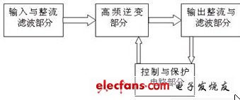
Figure 1 Block diagram of the switching power supply with normal mains as input
The input and rectification filtering part, the high frequency inversion part, and the output rectification and filtering part are the main sources of electromagnetic interference. The following is an analysis of the voltage and current waveforms of each part to clarify the cause of electromagnetic noise.
2.1 Electromagnetic noise caused by power frequency rectifier
Generally, the switching power supply is capacitive filtering, and the electromagnetic noise in the input and rectification filtering sections is mainly caused by current spikes and voltage fluctuations caused by the rectification process. After the sine wave power supply is subjected to differential mode and common mode signal attenuation by the power supply filter, the voltage obtained by the rectifier bridge rectification and electrolytic capacitor filtering is used as the input voltage of the high frequency inverter part. Due to the presence of the filter capacitor, the rectifier is not turned on for half a cycle like pure rectification, but only when the sinusoidal voltage is higher than the capacitor voltage, causing the current waveform to be very steep and the voltage waveform to be gentle. The waveforms of current and voltage are shown in Figure 2.
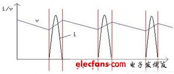
Figure 2 Current waveform through the rectifier and voltage waveform on the capacitor
According to the Fourier series, the current and voltage waveforms in the figure can be decomposed into a DC component and a series of sinusoidal AC components whose frequencies are integer multiples of the fundamental frequency. The electromagnetic field theory and experimental results show that harmonics (especially higher harmonics) can cause conducted and radiated interference. The interference formed by the propagation of the input and output lines of the switching power supply is called conducted interference, and the interference generated by the external electric field generated by the external magnetic field in the space is called radiation interference.
2.2 Electromagnetic noise caused by transformers and switch tubes
The inverter part is the core of the switching power supply, which is used to realize the transformation, frequency conversion and adjustment of the output voltage. It mainly consists of a switching tube and a high-frequency transformer. Electromagnetic noise is mainly caused by the leakage inductance of the transformer, the distributed capacitance, and the opening and closing of the switching tube. The high-frequency transformer in the switching power supply is used for isolation and voltage transformation. When the transformer is theoretically analyzed, it is generally considered to be an ideal transformer. However, in practical applications, the transformer has a leakage inductance, and in the case of high frequency, the transformer interlayer is also considered. Distributed capacitance. The equivalent circuit model of the high frequency transformer is shown in Figure 3.
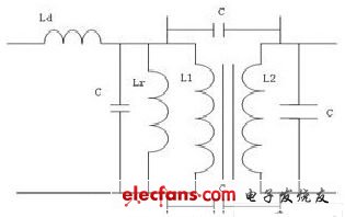
Figure 3 equivalent circuit model of high frequency transformer
It can be seen from the figure that the distributed capacitance between the transformer layers makes the high frequency noise in the switching power supply easily transfer between the primary and secondary. Moreover, if the capacitance of the capacitor is insufficient or the high-frequency characteristics are not good, the high-frequency impedance on the capacitor causes the high-frequency current to pass through the parasitic capacitance of the transformer to the AC power source in a differential mode.
The fundamental reason for the reduction in the size and weight of the switching power supply is to operate the power semiconductor device in a high frequency switching state, but the result is a very serious electromagnetic interference. The reason is high di/dt and dv/dt during the working process, as well as transformer leakage inductance, high frequency oscillation between the parasitic inductance of the circuit and the parasitic capacitance of the switching transistor. The voltage waveforms in the switching power supply are mostly periodic waves close to a rectangle, such as the driving waveform of the switching transistor and the MOSFET drain-source voltage waveform. The frequency is high, generally above kHz, the rise and fall times are short, dv/dt is large, and after the Fourier expansion, the harmonic frequencies involved are very high, and it is easy to pollute the surrounding electromagnetic environment.
Switching tubes (such as MOSFETs) can also cause strong electromagnetic interference when turned on and off. Due to the leakage inductance of the primary coil of the transformer, the parasitic inductance of the circuit causes a part of the energy to be transmitted from the primary side to the secondary side. The energy is stored in the leakage inductance, and the current suddenly changes when the power is turned off, and the di/dt is very high, generating a counter electromotive force. It is known from the electromagnetic field theory that E=-Ldi/dt.
Its value is proportional to the change in current and proportional to the inductance. Therefore, the leakage inductance will produce a very high back electromotive force superimposed on the turn-off voltage, forming a turn-off voltage spike, causing conductive electromagnetic interference. The leakage inductance and the parasitic capacitance between the switching tubes may also oscillate, affecting the electromagnetic environment in the circuit and generating noise. When the switch is turned on, the parasitic capacitance is instantaneously discharged, causing a spike current, and the primary coil also causes a surge current to be generated, which affects the electromagnetic environment.
2.3 Output Rectifier Diode Reverse Recovery Caused by Electromagnetic Noise
When the diode is subjected to a reverse voltage, the accumulated charge in the PN junction will be released and form a reverse current. The magnitude, pulse width and shape of the reverse recovery current pulse are related to the characteristics of the diode itself and the circuit parameters, and the time to return to zero. Related to factors such as junction capacitance. Due to the large amplitude and di/dt of the reverse recovery current pulse, the high-frequency rectifier diode generates a high induced voltage in the lead inductance and the circuit connected thereto, resulting in a very wide-band transient electromagnetic noise. The voltage and current waveforms of the diode reverse recovery process are shown in Figure 4.

Figure 4 diode reverse recovery process voltage, current waveform
Fast recovery diodes are used in converter circuits with high switching frequency, such as high-frequency switching power supplies, high-frequency DC/DC resonant converters, and power factor correction circuits. Their reverse recovery time is usually on the order of nanoseconds, so transient electromagnetic noise caused by lead inductance is not negligible. Especially in the flyback switching power supply, the diode reverse recovery current spike may also pass from the secondary to the primary. When the switch is turned on, a current spike is formed, which not only easily burns the switching tube but also causes electromagnetic noise.
Feature:
1.Superior uniformity and EV grade safefty LFP battery ;
2.Customized modular and large-scale ESS solution;
3.Reliable safety design and remote real-time monitoring;
4.High cost effective and short delivery duration.
ESS Energy Storage System,mwh,ess container, bess,commercial battery,battery container,mega,megawatt
Shenzhen Enershare Technology Co.,Ltd , https://www.enersharepower.com