Microchip's PIC32MZ EF series is a 250MHz integrated floating point unit (FPU) with a wide range of peripherals and excellent connectivity options including local area network (CAN), operating voltages from 2.1V to 3.6V, and DSP enhanced cores with four 64-bit accumulator, single-cycle MAC, and IEEE 754 compatible, mainly used in demanding automotive and industrial applications such as high-resolution audio. This article describes the main features of the PIC32MZ EF series, block diagram, processor core MIPS32® M-Class Key features and main features and schematics and bill of materials for the PIC32MZ EF Curiosity development board.
The PIC32MZ EF family features high core performance up to 250 MHz, an integrated FloaTIng-Point Unit (FPU), a wide selecTIon of peripherals and excellent connecTIvity opTIons including Controller Area Network (CAN). The Extended temp portfolio is ideal for several critical automotive And industrial applications that require reliable performance and robustness at higher temperatures.
In addition, the industrial temperature portfolio (-40°to 85°C) has been selectively expanded to offer a higher-speed variant (250 MHz/795 CoreMark®). The high-speed variant is ideal for applications like high-resolution audio that Requires slightly higher core performance to provide faster audio processing and streaming.
Key features of the PIC32MZ EF series:
Operating Conditions
• 2.1V to 3.6V, -40°C to +85°C, DC to 252 MHz
• 2.1V to 3.6V, -40°C to +125°C, DC to 180 MHz
Core: 252 MHz (up to 415 DMIPS) M-Class
• 16 KB I-Cache, 4 KB D-Cache
• FPU for 32-bit and 64-bit floating point math
• MMU for optimum embedded OS execution
• microMIPSTM mode for up to 35% smaller code size
• DSP-enhanced core:
-Four 64-bit accumulators
-Single-cycle MAC, saturating, and fractional math
-IEEE 754-compliant
• Code-efficient (C and Assembly) architecture
Clock Management
•Programmable PLLs and oscillator clock sources
• Fail-Safe Clock Monitor (FSCM)
• Independent Watchdog Timers (WDT) and Deadman Timer (DMT)
• Fast wake-up and start-up
Power Management
•Low-power modes (Sleep and Idle)
• Integrated Power-on Reset (POR) and Brown-out Reset (BOR)
Memory Interfaces
• 50 MHz External Bus Interface (EBI)
• 50 MHz Serial Quad Interface (SQI)
Audio and Graphics Interfaces
•Graphics interfaces: EBI or PMP
• Audio data communication: I2S, LJ, and RJ
• Audio control interfaces: SPI and I2C
•Audio master clock: Fractional clock frequencies with USB synchronization
High-Speed ​​(HS) Communication Interfaces (with Dedicated DMA)
• USB 2.0-compliant Hi-Speed ​​On-The-Go (OTG) controller
• 10/100 Mbps Ethernet MAC with MII and RMII interface
Security Features
• Crypto Engine with RNG for data encryption/decryption and authentication (AES, 3DES, SHA, MD5, and HMAC)
• Advanced memory protection:
-Peripheral and memory region access control
Direct Memory Access (DMA)
•Eight channels with automatic data size detection
•Programmable Cyclic Redundancy Check (CRC)
Advanced Analog Features
• 12-bit ADC module:
-18 Msps with up to six Sample and Hold (S&H) circuits (five dedicated and one shared)
-Up to 48 analog inputs
-Can operate during Sleep and Idle modes
-Multiple trigger sources
-Six Digital Comparators and six Digital Filters
• Two comparators with 32 programmable voltage references
•Temperature sensor with ±2oC accuracy
Communication Interfaces
• Two CAN modules (with dedicated DMA channels):
-2.0B Active with DeviceNetTM addressing support
• Six UART modules (25 Mbps):
-Supports up to LIN 2.1 and IrDA® protocols
• Six 4-wire SPI modules (up to 50 MHz)
• SQI configurable as an additional SPI module (50 MHz)
• Five I2C modules (up to 1 Mbaud) with SMBus support
• Parallel Master Port (PMP)
• Peripheral Pin Select (PPS) to enable function remap
Timers/Output Compare/Input Capture
• Nine 16-bit or up to four 32-bit timers/counters
• Nine Output Compare (OC) modules
• Nine Input Capture (IC) modules
•Real-Time Clock and Calendar (RTCC) module
Input/Output
• 5V-tolerant pins with up to 32 mA source/sink
•Selectable open drain, pull-ups, pull-downs, and slew rate controls
•External interrupts on all I/O pins
•PPS to enable function remap
Qualification and Class B Support
• AEC-Q100 REVH (Grade 1 -40oC to +125oC)
• Class B Safety Library, IEC 60730 (planned)
• Back-up internal oscillator
Debugger Development Support
•In-circuit and in-application programming
• 4-wire MIPS® Enhanced JTAG interface
•Unlimited software and 12 complex breakpoints
• IEEE 1149.2-compatible (JTAG) boundary scan
• Non-intrusive hardware-based instruction trace
Software and Tools Support
• C/C++ compiler with native DSP/fractional and FPU support
•MPLAB® Harmony Integrated Software Framework
•TCP/IP, USB, Graphics, and mTouchTM middleware
• MFi, AndroidTM, and Bluetooth® audio frameworks
• RTOS Kernels: Express Logic ThreadX, FreeRTOSTM, OPENRTOS®, Micriμm® μC/OSTM, and SEGGER embOS®
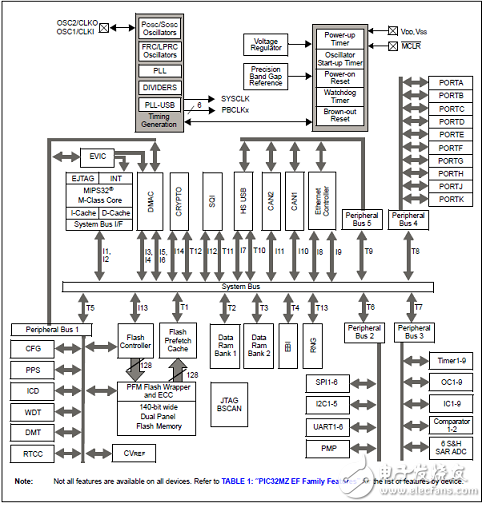
Figure 1. PIC32MZ EF Series Block Diagram
PIC32MZ EF Series Processor Core MIPS32® M-Class
The MIPS32® M-Class Core is the heart of the PIC32MZ EF family device processor. The CPU fetches instructions, decodes each instruction, fetches source operands, executes each instruction and writes the results of instruction execution to the proper destinations.
Main features of the processor core MIPS32® M-Class:
• 5-stage pipeline
• 32-bit address and data paths
• MIPS32 Enhanced Architecture (Release 5):
-Multiply-accumulate and multiply-subtract instructions
-Targeted multiply instruction
-Zero/One detect instructions
-WAIT instruction
-Conditional move instructions (MOVN, MOVZ)
-Vectored interrupts
-Programmable exception vector base
-Atomic interrupt enable/disable
-GPR shadow registers to minimize latency for interrupt handlers
-Bit field manipulation instructions
-Virtual memory support
• microMIPSTM compatible instruction set:
-Improves code size density over MIPS32, while maintaining MIPS32 performance.
-Supports all MIPS32 instructions (except branch-likely instructions)
-Fifteen additional 32-bit instructions and 39 16-bit instructions corresponding to commonly-used MIPS32 instructions
-Stack pointer implicit in instruction
-MIPS32 assembly and ABI compatible
• MMU with Translation Lookaside Buffer (TLB) mechanism:
-16 dual-entry fully associative Joint TLB
-4-entry fully associative Instruction and Data TLB
-4 KB pages
• Separate L1 data and instruction caches:
-16 KB 4-way Instruction Cache (I-Cache)
-4 KB 4-way Data Cache (D-Cache)
• Autonomous Multiply/Divide Unit (MDU):
-Maximum issue rate of one 32x32 multiply per clock
-Early-in iterative divide. Minimum 12 and maximum 38 clock latency (dividend (rs) sign extension-dependent)
• Power Control:
-Minimum frequency: 0 MHz
-Low-Power mode (triggered by WAIT instruction)
-Extensive use of local gated clocks
• EJTAG Debug and Instruction Trace:
-Support for single stepping
-Virtual instruction and data address/value breakpoints
-Hardware breakpoint supports both address match and address range triggering.
-Eight instruction and four data complex breakpoints
• iFlowtrace® version 2.0 support:
-Real-time instruction program counter
-Special events trace capability
-Two performance counters with 34 user-selectable countable events
-Disabled if the processor enters Debug mode
-Program Counter sampling
• Four Watch registers:
-Instruction, Data Read, Data Write options
-Address match masking options
• DSP ASE Extension:
-Native fractional format data type operations
-Register Single Instruction Multiple Data (SIMD) operations (add, subtract, multiply, shift)
-GPR-based shift
-Bit manipulation
-Compare-Pick
-DSP Control Access
-Indexed-Load
-Branch
-Multiplication of complex operands
-Variable bit insertion and extraction
-Virtual circular buffers
-Arithmetic saturation and overflow handling
-Zero-cycle overhead saturation and rounding operations
• Floating Point Unit (FPU):
-1985 IEEE-754 compliant Floating Point Unit
-Supports single and double precision datatypes
-2008 IEEE-754 compatibility control of NaN handling and Abs/Neg instructions
-Runs at 1:1 core/FPU clock ratio
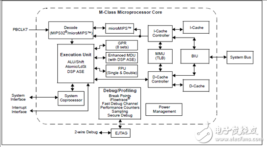
Figure 2. Processor core MIPS32® M-Class block diagram
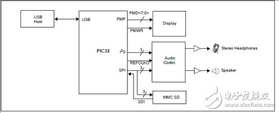
Figure 3. PIC32MZ EF Audio Player Application Block Diagram
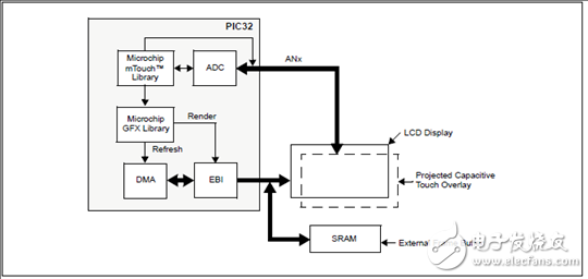
Figure 4. PIC32MZ EF low-cost controllerless (LCC) image application block diagram for capacitive touch
PIC32MZ EF Curiosity Development Board
The PIC32MZ EF Curiosity Development Board includes an integratedprogrammer/debugger and requires no additional hardware to get started. Userscan expand functionality through MikroElectronikamikroBUSTM ClickTM adapterboards, add Ethernet connectivity with the Microchip LAN8720A PHY DaughterBoard, add Wi-FiTM connectivity using the Microchip MRF24WN0MA On-board Wi-Fimodule, and add audio input/output capability with Microchip audio daughterboards.
With or without expansion boards, the PIC32MZ EF Curiosity Development Boardprovides the freedom to develop for a variety of applications, including Internet ofThings (IoT), robotics development, and proof-of-concept designs.
The PIC32MZ EF Family Starter Kit contains the following items:
• One PIC32MZ EF Curiosity Development Board
• One on-board PIC32MZ2048EFM100 microcontroller
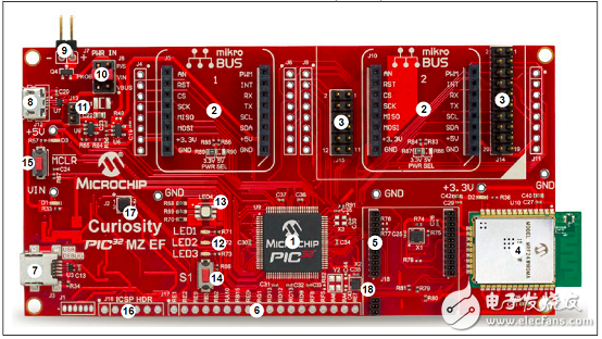
Figure 5. Outline of the PIC32MZ EF Curiosity Development Board
Figure 5 Digital counterparts in the PIC32MZ EF Curiosity development board:
1. PIC32MZ2048EFM100 32-bit microcontroller (U9).
2. Two mikroBUS sockets to expand functionality using MikroElectronika Clickadapter boards (J5, J10).
3. X32 header for audio I/O using Microchip audio daughter boards (J14, J15).
4. MRF24WN0MA, 2.4 GHz IEEE 802.11n compliant wireless module (U10).
5. Header for flexible Ethernet PHY options using Microchip PHY daughter boards (J18).
6. GPIO expansion header (J17).
7. Debug USB connector for programming/debugging (J3).
8. Target USB connector for PIC32 USB connectivity (Device/Host mode) (J12).
9. Header for external 5V input (J7).
10. Jumper to select power source: Debug USB connector, target USB connector and external +5V input (J8).
11. Jumper to drive VBUS in Host mode (J13).
12. Three user LEDs (LED1, LED2, and LED3).
13. RGB LED (LED4).
14. User button (S1).
15. Reset Button (MCLR).
16. ICSP header for external debugger, such as MPLAB® REAL ICETM or MPLABICD 3 (J16).
17. Jumper to select on-board debugger or external debugger (J2).
18. 24 MHz crystal oscillator (X2).
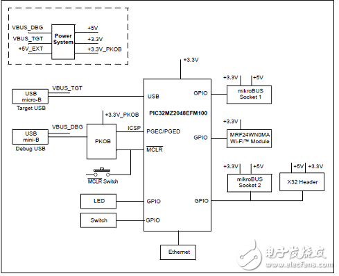
Figure 6. Block diagram of the PIC32MZ EF Curiosity development board
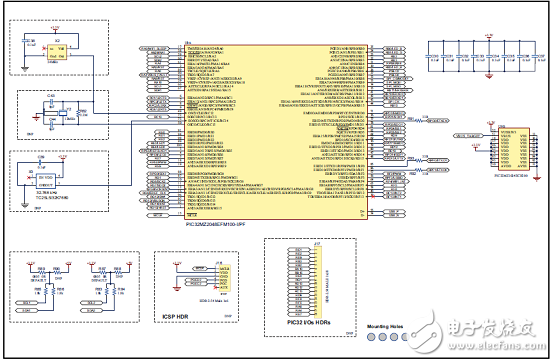
Figure 7. PIC32MZ EF Curiosity Development Board Circuit Diagram (1)
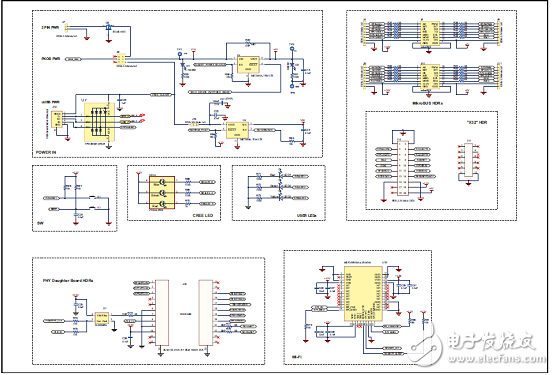
Figure 8. PIC32MZ EF Curiosity Development Board Circuit Diagram (2)
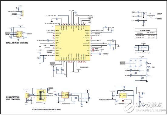
Figure 9. PIC32MZ EF Curiosity Development Board Circuit Diagram (3)
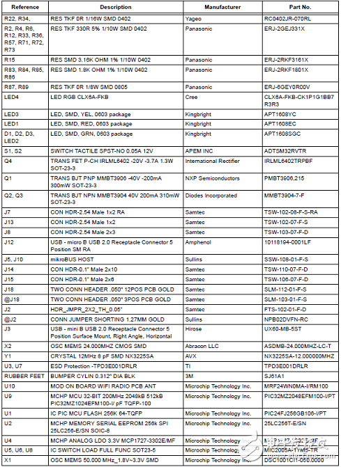
PIC32MZ EF Curiosity Development Board Bill of Materials:
Car Audio Harness,Stereo Wiring Harness,Car Stereo Wiring Harness,Car Stereo Wiring
Dong guan Sum Wai Electronic Co,. Ltd. , https://www.sw-cables.com