How many wafers can a wafer be cut? This is determined by the size of your die and the size of the wafer and the yield. The so-called 6-inch, 12-inch or 18-inch wafers in the industry are actually short for wafer diameter, but this is an estimate.
The actual wafer diameter is divided into three types: 150mm, 300mm, and 450mm, and 12å‹ is equal to 305mm. It is called a 12-inch wafer for convenience.
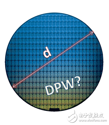
The general calculation formula of the international Fab factory:

Smart readers must have found that the square of π* (wafer diameter/2) in the formula is not the formula of the circular area? If you simplify the formula, it will become:
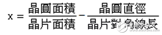
X is the so-called dpw die per wafer.
Then come to test your computing skills!
Assuming that the 12-inch wafer costs $5,000 per piece, NVIDIA's latest GT200 wafer size is 576 square millimeters. At a yield of 50%, what is the average cost per dollar?
Answer: USD.87.72
In order to make the calculation easier, click on the original to download the dedicated number calculator.
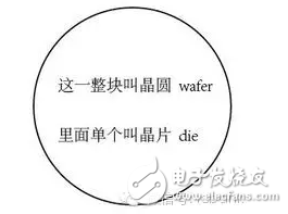
Popular science: the difference between wafer die
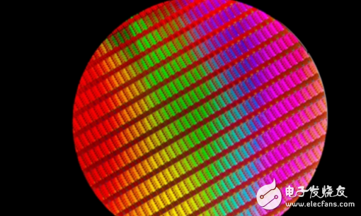
Let's start with a complete wafer (Wafer):
a complete wafer
Explanation of terms: wafer is the wafer shown in the picture, which consists of pure silicon (Si). Generally divided into 6-inch, 8-inch, and 12-inch specifications, the wafer is produced based on this wafer. A small piece on the Wafer is a wafer wafer body, named after the die, which becomes a particle after encapsulation. A wafer containing Nand Flash wafers, the wafer is first cut, then tested, and the intact, stable, full-capacity die is removed and packaged to form the Nand Flash chip that is seen everyday. Then, the rest on the wafer, or not, is unstable, or it is partially damaged, so it is not enough capacity, or it is completely damaged. The original factory considers the quality assurance, and will declare the death of this die, which is strictly defined as the scrapping of all waste products.
The relationship between die and wafer
After the qualified die is cut, the original wafer becomes the picture below, which is to pick the remaining Downgrade Flash Wafer.
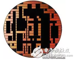
Filtered wafer
These residual die are actually wafers of unqualified quality. The part that is taken away, that is, the black part, is a qualified die, which will be packaged as a finished NAND granule by the original factory. The unqualified part, that is, the part left in the figure is treated as waste.
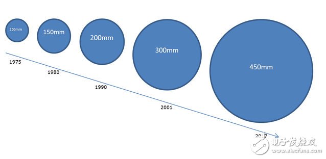
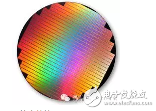
Wafer size development history (estimated)
Shenzhen Innovative Cloud Computer Co., Ltd. , https://www.xcypc.com