First, the design basis of class D audio power amplifier
D amplifier is a switching amplifier based on pulse width modulation technology, including pulse width modulator (hundreds of kilohertz switching frequency), power bridge circuit, low pass filter. This paper analyzes the basic issues related to the design of class D audio power amplifiers such as composition, topology comparison, MOSFET selection and power loss, distortion and noise generation, and audio performance, and cites Class D power amplifier reference designs.
1, the basic composition of the class D amplifier
There are many different types of power amplifiers, such as: Class A, Class B, Class AB, etc. But the difference between a class D amplifier is basically a switch power amplifier or a pulse width modulation power amplifier. To this end, the description of such Class D amplifiers will be mainly explained.
In this class D power amplifier, the device is either fully turned on or completely turned off, greatly reducing the power consumption of the output device, and an efficiency of 90-95% is possible. The audio signal is used to modulate the PWM carrier signal, the carrier signal can drive the output device, and the high-frequency PWM carrier frequency is removed with the final low-pass filter.
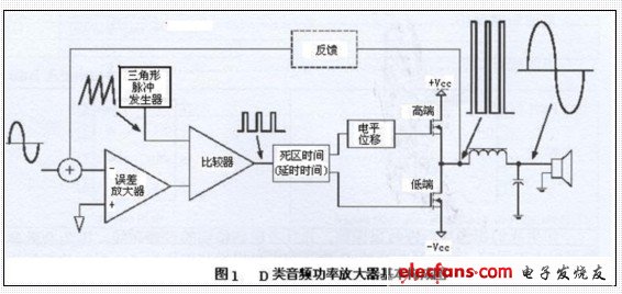
As we all know, Class A, Class B and Class AB amplifiers are linear power amplifiers. So what is the difference between Class D amplifiers and them? We should first discuss it. Figure 1 is a block diagram of the D power amplifier. In a linear power amplifier, the signal always stays in the analog area, and the output transistor (device) acts as a linear regulator to adjust the output voltage. This results in a voltage drop across the output device, which results in reduced efficiency.
Class D amplifiers come in many different forms, some are digital inputs, and some are analog inputs. Here we will focus on analog inputs.
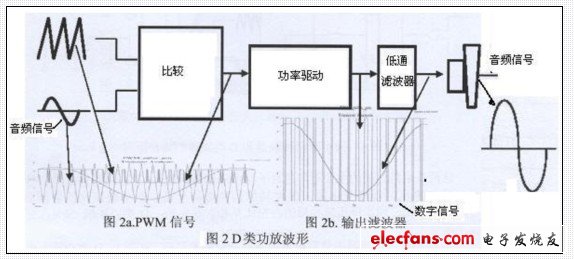
Figure 1 above shows the basic functional diagram of a half-bridge Class D amplifier, which shows the waveform for each stage. The circuit uses feedback from the half-bridge output to compensate for changes in the bus voltage. How does the Class D amplifier work? The Class D amplifier works the same way as the PWM power supply. We assume that the input signal is a standard audio signal, and this audio signal is a sine wave with a typical frequency ranging from 20 Hz to 20 kHz. This signal produces a PWM signal compared to a high frequency triangular or sawtooth waveform, as shown in Figure 2a. This PWM signal is used to drive the power stage to produce an amplified digital signal. The last low pass filter is used on this signal to filter out the PWM carrier frequency and regain the sine wave audio signal, as shown in Figure 2b.
2, from the topology comparison - see linear and D different
This will discuss the differences between linear power amplifiers (Class A and Class AB) and Class D digital power amplifiers. The main difference between the two is efficiency, which is why it is necessary to invent Class D amplifiers. Linear amplifiers have inherent linearity in terms of their performance, but even AB amplifiers are only 50% efficient, while Class D amplifiers are highly efficient, up to 90% in actual designs.
The gain-linear power amplifier gain is not affected by the bus voltage, however the gain of the Class D amplifier is proportional to the bus voltage. This means that the power disturbance rejection ratio of the Class D amplifier is 0 dB, and the linear PSRR (power supply rejection ratio) is good. Feedback is commonly used in Class D amplifiers to compensate for bus voltage variations.
Energy Flow - In a linear power amplifier, the energy is from the power source to the load, although this is also true in a full-bridge Class D power amplifier, but the half-bridge Class D power amplifier is different because the energy can flow in both directions, resulting in a "bus voltage boost" phenomenon. This will cause the bus capacitance to be charged from the loaded energy. This mainly occurs at low frequencies, such as below 100 Hz.
3, Class D power amplifier and Buck buck converter class topology difference
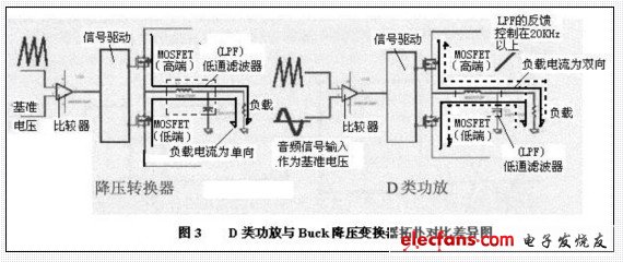
The topology principle of the class D power amplifier and synchronous buck converter is shown in Figure 3. The main difference between the two circuits is three: First, for a synchronous buck converter, the reference voltage comes from the slowly varying stable voltage of the feedback circuit; and the reference signal of the class D amplifier is an ever-changing audio signal. That is, the duty cycle of the synchronous buck converter is relatively stable, while the class D is constantly changing around the 50% duty cycle. Second, in the synchronous buck converter, the direction of the load current is always toward the load, that is, the inductor current is unidirectional, as shown in the left of Figure 3. However, in Class D power amplifiers, the current is in two directions, that is, the inductor current is bidirectional, as shown in the right side of Figure 3. The final difference is the way the MOSFET is optimized. Synchronous buck converters have different optimizations for high and low-end transistors. Longer periods require lower Rds(on), while shorter periods require lower Qg (gate charge), ie, the two switches function differently. . But Class D amplifiers have the same optimization for both MOSFETs. The high and low side devices have the same Ras(on), ie the two switches function the same.
4, the choice of MOSFET in class D power amplifier
A key factor in achieving high performance in a power amplifier is the switch in the power bridge circuit. The power loss, dead time and voltage, current transient glitch, etc. generated during the switching process should be minimized to improve the performance of the amplifier. Therefore, in this power amplifier, the switch requires a low voltage drop, fast switching time and low stray inductance.
Because of the fast switching speed of the MOSFET, it is your best choice for this power amplifier. It is a majority carrier device, which has a faster switching time than the IGBT and BJT, so it has better efficiency and linearity in the power amplifier. The choice of MOSFET is based on the power amplifier specifications. Therefore, before selecting the device, you must know the output power and load impedance (such as 100W 8Ω), power circuit topology (such as half bridge or full bridge), modulation degree (such as 89%-90%).
5, power loss in MOSFET
The loss in the power switch is quite different between the AB linear amplifier and the class D amplifier. First look at the losses in linear AB amplifiers, the losses can be defined as follows:
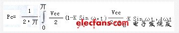
K is the ratio of the bus voltage to the output voltage.
For linear power amplifier power device losses, it can be simplified to the following formula:
It should be noted that the AB power amplifier power loss is independent of the output device parameters.
Now let's take a look at the loss of the Class D amplifier. The total loss in the output device is as follows:
Ptotal=Psw+Pcond+Pgd
Psw is switching loss
Pcond is the conduction loss,
Pgd is the gate drive loss
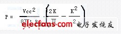
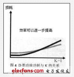
From the above equation, the output loss of the Class D power amplifier is determined according to the parameters of the device, that is, based on Qg (gate charge), Rds (on) (static drain-source on-state resistance), and Coss (output capacitance of the MOSFET). And tf (MOSFET fall time), so reduce the class D power amplifier loss should effectively select the device, Figure 4 is the power loss of the class D power amplifier and K as a function.
6. Comparison of half-bridge and full-bridge structure topologies
Similar to ordinary class AB amplifiers, class D amplifiers can be classified into two topologies, half-bridge and full-bridge. Each topology has its pros and cons. In short, the half bridge is simple, while the full bridge is better in audio performance. The full bridge topology requires two half-bridge amplifiers, which requires more components. Nonetheless, the bridge's inherent differential output structure eliminates harmonic distortion and DC offset, just as it does in an AB amplifier. A full-bridge topology allows for a better PWM modulation scheme, such as a three-level PWM scheme that quantifies almost no errors.
In a half-bridge topology, the power supply faces the energy returned from the amplifier and causes severe bus voltage fluctuations, especially when the amplifier outputs low frequency signals to the load. The return of energy to the power supply is a fundamental feature of Class D amplifiers. One arm in the full bridge tends to consume the energy of the other arm. So there is no energy that can be reflowed.
7, imperfect distortion and noise generation
An ideal Class D amplifier has no distortion, no noise in the audible band and 100% efficiency. However, the actual Class D amplifier is not perfect and will have distortion and noise. The imperfection is due to the distorted switching waveform generated by the Class D amplifier. Because:
* Nonlinearity in the PWM signal due to resolution limitations and time jitter from the modulator to the switching stage.
* Time error added to the gate drive, such as dead time, turn-on turn-off time, rise and fall time.
* Unnecessary features on the switching device, such as limiting resistance, limiting switching speed or body diode characteristics.
* Spurious parameters cause excessive edge oscillations.
* Power supply voltage fluctuation due to the limited output resistance and the reaction of the energy through the DC bus
* Outputs nonlinearity in LPF.
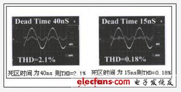
In general, the switching time error in the gate signal is the main cause of nonlinearity. In particular, the dead time has seriously affected the linearity of Class D amplifiers. A small dead time of tens of nanoseconds can easily produce more than 1% THD (total harmonic distortion), as shown in Figure 5(c).
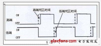
8. Dead time (see Figure 5(a) shows how nonlinearity is affected)
Figure 5(a)(b)(c) is a schematic diagram of the effect of dead time (or delay time) on distortion. The mode of operation in the Class D output stage can be categorized into three different regions depending on how the output waveform follows the input time. In these three different work areas, the output waveform follows the different edges of the high and low end input signals.
Let's examine the first operating region (see High Side edges, see Figure 5c), where the output current flows from the Class D amplifier to the load when the current is greater than the inductor ripple current. The high-side device is turned off before the low-side device turns on, and the output node is turned to the negative bus. This process is independent of the low-side device turn-on time, which is automatically caused by the commutation current from the demodulating inductor. Therefore, the output waveform is independent of the dead time embedded in the low-side device before it is turned on. Therefore, the PWM waveform is only shorted by the dead zone embedded in the high side gate signal, resulting in a slight voltage gain reduction of the desired input duty cycle.
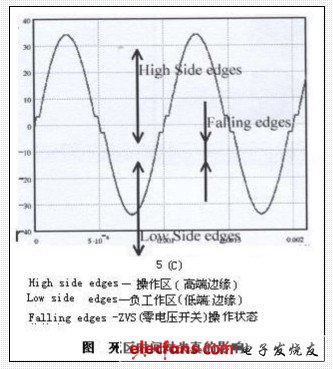
A similar situation occurs in the negative working area (see Low side edges in Figure 5c), and the output current flows from the load to the Class D amplifier. The current is higher than the inductor ripple current. In this case, the time of the output waveform is not affected by the dead time embedded in the high-side turn-on edge, and the low-end input time is always allowed. Therefore, the PWM waveform is only short-circuited by the dead time embedded in the low-side device gate signal.
In the two modes of operation previously described, there is an area in which the output time is independent of the dead time. When the output current is less than the inductor ripple current, the output time follows the turn-off edge of each input. Because in this area, it is the ZVS (Zero Voltage Switching) operating state (see Falling edges shown in Figure 5c), there is no distortion in the middle area.
When the output current varies with the audio input signal, the Class D amplifier will change its operating region so that each has a small, different gain. The three different regions in the period of the audio signal increase the parliament to distort the output waveform.
Figure 5(b) shows how dead time affects THD performance. A 40nS dead time can produce 2% THD. This can be increased to 0.2% by reducing the dead time to 15nS. This marks the importance of better linearity and high-low-side switching device conversion processes.
9, audio performance measurement
Audio measuring instruments with AESl7 network filters are required. Of course, like the traditional audio analyzer HP8903B, plus a suitable pre-stage low-pass filter can also be used. An important consideration here is that the output signal of the Class D amplifier still contains a large amount of switching carrier frequency on its waveform, which causes erroneous reading. These analyzers may be difficult to prevent carrier leakage from Class D amplifiers.
10, prevent straight through
Still, a narrow dead time is dangerous in mass production. Because once the high and low side transistors are turned on at the same time, the voltage of the DC bus will be shorted by the transistor, and a large amount of through current will start to flow, which will cause damage to the device. We should note that the effective dead time is different for each amplifier, related to component parameters and chip temperature. For a reliable design of a Class D amplifier, it is important to ensure that the dead time is always positive and never negative to prevent the transistor from entering the pass.
11, about the power absorption energy
Another reason for the significant derating in Class D amplifiers is bus charging, which can be seen when the half-bridge topology is outputting low frequencies to the load. Always remember that the gain of a Class D amplifier is directly proportional to the bus voltage. Therefore, the bus voltage fluctuations cause distortion, and the current flow in the class D power amplifier is bidirectional, and there is a period from the power amplifier returning to the power supply. The amount of energy that flows back into the power supply comes from the energy stored by the inductor of the output LPF. Often, there is no way for the power supply to absorb the energy that flows back from the load. Therefore, the bus voltage rises, causing voltage fluctuations. The bus voltage rise does not occur on the full bridge topology because the energy from the switch bridge to the source is consumed by the other bridge arm.
12. Consideration of EMI (electromagnetic radiation)
EMI (electromagnetic radiation) in D-amp design is cumbersome, as in other switching applications. One of the main sources of EMI is the reverse recovery charge from MOSFET diodes flowing from high to low, which is very similar to current through. The inductor current in the output LPF turns on the body diode during insertion into the dead zone that blocks the shoot-through current. In the next stage, when the MOSFET at the other end is not turned on in the dead zone, the body transistor remains on unless a large number of stored carriers are fully recombined. This reverse recovery current tends to form a very pointed shape, and due to the desired oscillation of the PCB board and package stray inductance due to the start. Therefore, PCB layout design is critical to reducing EMI and system reliability.
13. Other considerations for MOSFET selection in Class D amplifiers
* Choose the right package and structure
* The THD, EMI and efficiency of the amplifier are also affected by the body diode of the FET. Shorten body diode recovery time (FET of parallel Schottky diodes of R); reduce reverse recovery current and charge, improve THD; EMI and efficiency.
* FET crust thermal resistance should be as small as possible to ensure that the junction temperature is below the limit.
* Guaranteed better reliability and low cost conditions, working at maximum junction temperature. Whether the device encapsulated with insulation is directly mounted or insulated with a bare backplane structure depends on its cost and size.
14, Class D power amplifier reference design shown in Figure 6.
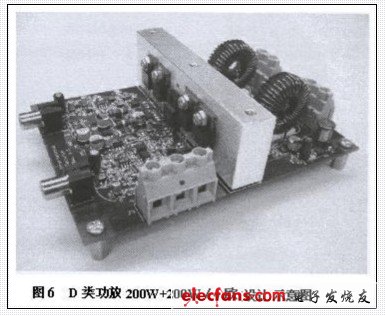
*Topology: Half Bridge
*Use IR2011S (gate drive IC, maximum working voltage 200V, Io+/- 1.0A/1.0A, Vout 10-20V, ton/off 80&60ns, delay matching time 20ns); IRFB23N15D (MOSFET power tube ID =23A, R DS=90mΩ, Qg=37nC Bv=150V To-220 package)
*Switching frequency: 400KHz (adjustable)
*Rated output: 200W+200W/4 ohms
*THD: 0.03%-1mhz half power
* Frequency response: 5Hz-40KHz (-3dB)
*Power supply: ~220v±50V
*Size: 4.0 "&TImes; 5.5"
15. Conclusion
If we are careful when choosing a device, and considering the fine design wiring, because the spurious parameters have a great impact, the current efficient Class D amplifier can provide similar performance to the traditional Class AB amplifier.
Shenzhen GEME electronics Co,.Ltd , https://www.gemesz.com