This article is the author's experience in the PSR primary feedback power supply design for many years. This chapter will continue to share the EMC design skills in the PSR primary feedback power supply, hoping to help everyone's actual design.
Let me talk about PCBLAYOUT points:
Everyone knows that EMC has to pay attention to the ground wire. The primary ground wire for PSR can be divided into four ground lines, as shown in the triangle symbol. These four ground lines need to adopt a "one-point grounding" layout.
First on the circuit diagram:
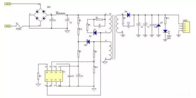
1. The ground wire of C8 is the power input ground.
2. The ground of R5 is power ground.
3. The ground of C2 is a small signal ground.
4. The ground of transformer PIN3 is shielded.
The junction of these four grounds is the negative end of C8, that is, the input voltage passes through the rectifier bridge and passes through C1 to C8. The ground of R5 and transformer PIN3 are directly connected to the negative end of C8 by separate wiring, and the connection is as short as possible; The R5 ground wire should be as wide as possible due to the consideration of voltage drop and interference.
The C5, R10, U1PIN7 and PIN8 ground lines are combined to cause the C2 negative terminal to be connected to the C8 negative terminal.
If it is a double panel, the above four ground wires should not be connected by via holes as much as possible. It is not allowed to use multiple via arrays to reduce the via voltage drop.
The above ground wire layout is appropriate, and the common mode interference of the product will be small.
Due to the DCM mode in the PFM state when the PSR line is loaded, the DI/DT is increased and the frequency is increased. Therefore, it is difficult to handle the 150K~5M differential mode interference.
According to the figure, the components affecting EMC are analyzed one by one from left to right.
Fuse
Switching the fuse to the fuse resistor theoretically has a negative impact on product efficiency, but the actual performance is not obvious.
Therefore, the fuse can use the 10/1W fuse resistor to reduce the differential mode interference near 150K, which has no significant impact on the energy consumption through the 5th grade, and the cost is also reduced.
2.C1, L2, C8
The PSR works in DCM mode, and its input peak current is much larger, so input filtering is important.
The increase in peak current will result in a lower bus voltage at low voltage input and an increase in the temperature rise of C8;
In order to increase the bus voltage and reduce the temperature rise of C8, it is necessary to increase the capacity of C1 and use C1 and C8 of LOWESR.
Since the operating voltage of C1 and C8 will increase after the capacity of C1 is increased, the peak current of the input will decrease with the same output power.
Due to the effect of L2, the actual performance of increasing the capacity of C1 is more effective than increasing the capacity of C8 to suppress EMC.
Generally, C1 is 6.8uF, and C8 is 4.7uF. If it is limited by space, it is better to use 8.2u and 3.3u than to use two 2.7u EMC suppression effects.
L2 generally uses color-ring inductance from the cost consideration. Because the power of the color-ring inductor is limited, the inductance is too large, which will seriously affect the efficiency. Generally, it takes 330u~2mH.
2mH is the effect of efficiency becoming obvious, 330u is not enough for differential mode interference. In order to minimize the effect of efficiency and better suppression of differential mode interference, it is recommended to use 1mH.
Because the "one-point ground" layout is concentrated at the negative end of C8, the direction of the input current at the negative terminal of C8 is flowed back to the input through C1 and BD1. According to the principle of conduction test, this has a negative effect, so it needs to be in C1 and C8. The ground wire is processed. If there is space, the magnetic bead jumper can be added in the middle. The space limitation can be realized by the PCBlayout curve. Although the effect will be weaker, it will be improved compared with the straight line connection.
3.R6, D2, R2, C4
Everyone should have already understood the impact of RCD absorption on EMC. Here we mainly talk about the impact of R6 and D2 on EMC.
The addition of R6 and D2 use a slower recovery time 1N4007 has a certain negative effect on space radiation, but is beneficial for conduction.
Therefore, when the EMC is rectified, the changes here have to pay attention to the choice of space radiation and conduction.
4.R5
R5 is both a current sense point and a power limit set point.
Therefore, the value of R5 will affect the peak current and also affect the OPP protection point.
It is recommended to take as much as possible when the OPP is satisfied.
Generally not less than 2R, it is recommended to take 2.2R.
5.R4, R10, D3, R3, C2
In the previous section, it was mentioned that the increase in VCC voltage has a malignant effect on EMC. Since the internal detection of the IC uses an integration circuit, when the VCC voltage is set too high, a longer integration time is required. When the period is constant, the TON time is increased, and the output power is constant. The peak current will increase, and the peaks at R7 and C11 of RCD and D4 will increase, and D3, R3, and C2 will also pull down and absorb VCC, which will increase the overshoot of the output voltage and affect the delay detection. Opening time. The impact of this series of changes on EMC cannot be ignored.
According to experience, combined with the leakage inductance of the transformer, the maximum value of the VCC voltage at full load should not exceed 19V. Therefore, in order to make the VCC not too low, the VCC voltage is designed to be 15V, and the leakage inductance of the transformer should not exceed 15%. .
6.C5
C5 is the IC internal delay detection compensation setting terminal. If the value of C5 is large, the period of voltage detection will be lengthened. If it is small, the period of voltage detection will be shortened. The change of the detection period will affect the sampling rate of the voltage, and it will also affect the current ripple throughout the product, which will also have a certain impact on EMC. Generally, 0.01~0.1uF is selected.
7.C3, C7
As mentioned above, the capacity values ​​of C3 and C7 suppress the output voltage overshoot and maintain the stability of the product. However, the capacity of C3 and C7 is not as large as possible, and it will have a negative effect on EMC. The increase in C3 and C7 capacity will also lead to an increase in the peak current mentioned in point 5, so it cannot be blindly selected.
The experience of designing and debugging the PSR primary feedback control switching power supply has come to an end, and I hope to bring help to everyone's actual design.
Dc Cross-Flow Fan,Dc Axial Fans,Dc Cross Flow Blower,Dc Cross Flow Fan
Original Electronics Technology (Suzhou) Co., Ltd. , https://www.original-te.com