Abstract: This paper takes DSP as the core processor, cooperates with FPGA and peripheral circuits, and designs a set of photoelectric tracking measurement system infrared TV focusing controller, which realizes the automatic adjustment of TV focal length according to parameters such as target distance and ambient temperature. Through data analysis and practice testing, the system can meet the focus control requirements of infrared TV.
1 Introduction
With the rapid development of infrared imaging technology, infrared measurement television has become an important part of the photoelectric tracking system. The automatic and continuous focusing of the infrared camera is the key technology to ensure the quality of infrared TV imaging and realize high-precision and stable tracking of the photoelectric tracking system. In general, there are many factors affecting infrared TV imaging, and the parameters such as the distance of the target and the ambient temperature have a great influence on the imaging quality. How to adjust the position of the camera in real time according to the information of the target image quality such as the target distance and the ambient temperature. In order to obtain a clear target image, extensive and in-depth research is needed, which is of great significance for realizing the stable and high-precision tracking measurement function of the infrared tracking measurement system.
2. Focusing controller hardware design
2.1 Overall structure and principle
Photoelectric tracking measurement system The functions to be realized by the focus control system include: receiving the control commands of the integrated controller, realizing the zooming and focusing functions of the infrared TV, combining the self-checking function and fault diagnosis capability, and fault diagnosis to the circuit board.
The system uses a DSP+FPGA based dimming focus controller. The hardware block diagram of the controller is shown in Figure 1.
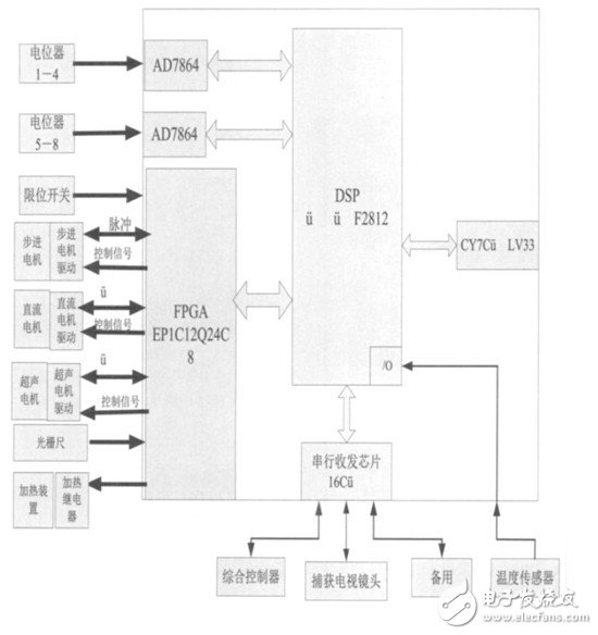
Figure 1 Dimming focus controller hardware block diagram
Among them DSP (TMS320F2812) as the core of the dimming focus controller. TMS320F2812 is TI's digital control field. It is the highest performance processor in the control field. It has the advantages of high control precision, fast speed, flexible use and high integration. It has been widely used in industrial automation, optical network and automation. Control and other fields.
The system uses EP1C12Q240C8 in Cyclone series FPGA as the timing and logic control core of the whole dimming focus controller. EP1C12Q240C8 provides 12060 logic units (LE) and 173 I/O ports, which can embed 4K RAM.
Apply part of all TMS320F2812 peripheral interfaces, such as GPIO interface and EVA/EVB interface.
With programmable logic devices (FPGAs), the hardware circuitry of the DSP can be designed very simply. The DSP data bus, address bus, read and write control lines, and interrupt signal lines are all introduced into the FPGA, and timing and logic design are completed in the FPGA according to specific requirements. Among them, TL16C554, AD7864 provides address strobe signal, providing quadruple frequency phase discrimination and counting logic for grating scale calculation.
Since the number of signal lines and limit switch lines of the motor is large, the number of I/O ports of the system needs to be large, and the function of expanding the I/O port can be completed in the FPGA.
2.2 FPGA design
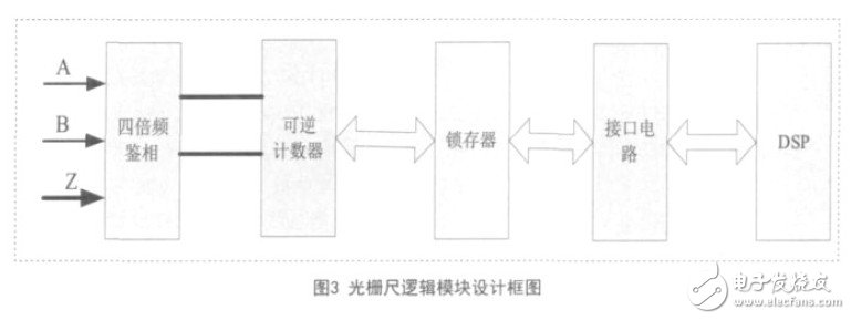
The FPGA uses modular design ideas to decompose the FPGA design. It mainly includes the functions of implementing FPGA extended I/O port, providing chip selection and read/write signals for TL16C554 and AD7864, providing quadruple frequency phase discrimination and counting logic to calculate the position of the scale. The functional modules in the FPGA are shown in Figure 2.

TL16C554 address decoding module: In the FPGA, the DSP reads and writes and decodes the address signal, and provides signals for reading and writing signals and chip selection for the TL16C554.
AD7864 address decoding module: decodes the address signal of DSP, and provides signals for reading, writing, chip selection and channel selection for AD7864.
The grating rule logic calculation module: the grating scale outputs two orthogonal square wave signals A, B and zero bit signal Z input into the FPGA, realizes the frequency multiplication and phase discrimination function of the A and B signals in the FPGA, and then passes the 16 The bit counter and the latch are connected to the DSP, and the position value of the scale is obtained by reading the value of the counter. The system block diagram is shown in FIG.
Engine Start Up Battery,Engine Starter Battery Charger,Engine Start Battery,Engine Start Module
Langrui Energy (Shenzhen) Co.,Ltd , https://www.langruienergy.com