Keywords: CMX860, phone caller identification, phone tester
1 Introduction At present, with the general opening of the caller identification (caller ID) service in the telecommunications sector, phones with caller identification are becoming more and more popular. According to this situation, we have designed a multi-function telephone tester that can test the caller identification function. It uses CML (ConsumerMicrocircuit Limited) CMX860 as the core component of the caller ID test circuit, and the single chip uses SST89C58.
1.1 Introduction of CMX860 CMX860 is a general-purpose low-power telephone signaling transceiver IC. CMX860 contains DTMF codec, V. 23 modem, with functions such as ring current detection, off-hook detection, etc. It can be widely used in telephone equipment powered by lines.
The main features of CMX860 are: (1) Provide V. 23 1200 / 75bps FSK signal transmission and reception; (2) dual tone multi-frequency and audio signaling transmission and reception; (3) subscriber line end and telephone end driver; (4) call process decoding; (5) incoming call Waiting for signal generation and detection; (6) "C-BUS" serial bus interface; (7) Low power consumption working mode.
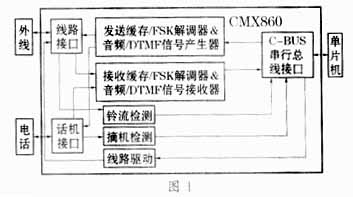
2 CMX860 and the connection of the one-chip computer A remarkable characteristic of CMX860 is that all its programming functions can be completed through a serial bus interface called C-Bus (C bus). The one-chip computer is connected with CMX860 through C-Bus, C-Bus serial bus can transmit the data, control or status information between the one-chip computer and CMX860 internal register.
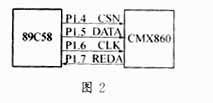
2. 1 CMX860 and the hardware connection of the one-chip computer C-Bus interface of CMX860 is compatible with most common one-chip computer serial interfaces, and can be connected with the one-chip I / O pin of the one-chip computer. This system uses P1.4, P1.5, P1.6, P1.7 of the P1 port of SST89C58 to connect with the C-Bus interface of CMX860. The specific connection is shown in Figure 2.
The functions of each pin of CMX860: CSN pin is used as enable pin, DATA pin receives serial data signal from MCU, CLK pin receives serial clock signal from MCU, REDA pin sends serial data signal to MCU.
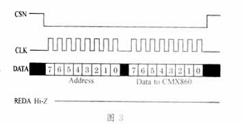
2.2 MCU programming CMX860 According to the timing of the C-Bus interface, at the rising edge of the serial input clock, the data sent from the MCU command data line is locked into the CMX860. When the serial clock is high, the response data sent from the CMX860 to the microcontroller is valid. During the data transfer, the CSN line (enable end) must be kept low, and high between the two transfers. In the specific transmission process, a byte sent by the microcontroller to the CMX860 first represents the CMX860 internal register address (see the reference [1] for the CMX860 internal register description and address), then, the write-only memory sent by the microcontroller to the CMX860 is one or more The data byte, or the one-chip computer reads one or more data bytes from the read-only memory of the CMX860, thereby completing the control programming of the CMX860. Figure 3 is a timing diagram of an address signal and a data signal sent from the microcontroller to the CMX860.
(1) The microcontroller writes a byte information subroutine to CMX860, and the information is stored in register A.
OUT BYTE: MOV R7, # 8
OUTB1: CLR CLK; the clock signal is set to low level
RLC A; read a bit from A?
MOV DATE, C; Put one bit of information into the DATA data line?
SETB CLK; the clock signal is set to low level
RLCA; read one bit from A
MOV DATE, C; put one bit of information on the DATA data line
SETB CLK; the clock signal is set to high level, the data on the DATA data line is sent to the CMX860 at the rising edge of the clock
DJNZR7, OUTB1; input a total of 8 bits CLR CLKRET
(2) The microcontroller reads a byte information subroutine from the CMX860, and the information is stored in the register A.
IN BYTE: MOV R7, # 8
INB1: CLR CLK; set the clock signal to low level?
NOP
SETBCLK; the clock signal is set to high level
MOV C, SOUT; read the data bits on the RDDA data line into the microcontroller when the clock signal is high
RLCA; store data bits in register A
DJNZR7, INB1; read 8 bits in total
CLR CLK
RET
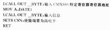
(3) The microcontroller writes a byte information subroutine to the CMX860 specific register.
WRITE BYTE: CLR CSN; set the enable terminal to low level MOV A, ADDR;
3 Introduction to Caller ID Identification
3.1 Caller identification service definition Caller identification information transmission and display service is a new service item provided to the called telephone, which means displaying the calling number, calling user name, Calling information such as the date and time of the call and storing it for users to consult.
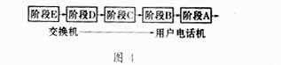
3.2 The method to realize caller identification The basic method to realize caller identification is that the originating switch transmits the calling number and other information to the terminal switch through the signaling system, and the terminal switch sends the caller identification information to dual tone multi-frequency (DTMF) or Frequency shift keying (FSK) is transmitted to the end user / terminal equipment. The terminal switch sends the caller identification information to the called user terminal between the first ringing and the second ringing.
3.3 Transmission timing of caller identification information data See Figure 4 for the transmission timing chart of caller identification information data.
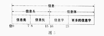
3.4 Calling identification information data format Calling identification information data consists of two parts: an information header and an information body. The information header is composed of an information type and an information length, both of which are 8 bits. The value of the information type is used to identify the type of information , The message length indicates the length of the subsequent message value, the message body includes the calling user information sent by the switch to the end user, the message body can accommodate 1 to 255 8-bit message words, and each word uses a ASCII code with check Said. As shown in Figure 5.
4 The hardware and software implementation of the caller ID test part in the telephone tester
4.1 Hardware implementation
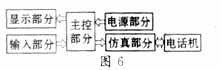
The caller ID test part of the telephone tester simulates the terminal switch to send the calling user information to the telephone under test to check whether the content displayed by the telephone under test is accurate. The principle block diagram is shown in Figure 6. Among them, the main control part includes SST89C58 and CMX860 and other circuits to generate and send calling user information; the power supply part provides + 5V and + 9V voltage to the main control part and the display part; the simulation part simulates the user loop of the exchange, connects the telephone, and sends The telephone provides 48V feed; the display part is used to display the status of the tester and various information such as the number sent by the phone to the tester; the input part is used to input the calling user information and the control commands of the tester.
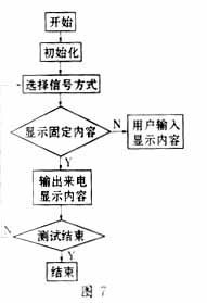
4.2 The software realizes that the system analog exchange sends caller identification information to the phone, and the phone displays the caller information after receiving it. The content of the caller identification information to be displayed can be obtained by two methods: (1) pre-stored in the data storage area during programming, this method can store all the content required by the national standard test; (2) input by the user, the user can Enter the information before the test as needed, which can increase the flexibility of the test. There are two signal methods for sending caller identification information: DTMF and FSK. The user can choose one or two signal modes according to the telephone under test. The test software flow chart is shown in Figure 7. The output of the caller ID information in the flow chart follows the flow of FIG. 4.
5 Conclusion We use CMX860 as the core design of a multi-function telephone test system that can test the caller ID, which has been put into use.
2 He Limin. MCS-51 series microcontroller application system design. Beijing: Beijing University of Aeronautics and Astronautics Press, 1990
3 Sun Hanfang, Xu Aiqing. MCS-51, 96 series single-chip microcomputer principle and application. Beijing: Beijing University of Aeronautics and Astronautics Press, 1988
test discord discord discord discord discord discord test discord discord discord discord discord discord test discord discord discord discord discord discord test discord discord discord discord discord discord test discord discord discord discord discord discord kh
2222Bossgoo(China)Tecgnology.(Bossgoo(China)Tecgnology) , https://www.cn-gangdao.com