The FSK technology with strong anti-interference ability is used to form the inductive communication system. The coupling coil is used to realize the wireless communication between the drill pipes. The inside of the drill pipe uses the coaxial cable to transmit information, so that a higher data bit rate can be obtained. In this paper, the AT89C51 single-chip microcomputer is used as the control system, and a set of FSK system that can realize two-way communication is designed. The reliability and bit error rate of the system are tested.
Oil and natural gas are the natural resources for human survival. In the process of drilling and mining, real-time understanding of the high temperature and high pressure environment is needed, so the real-time requirements for signal transmission are very high. However, the underground environment is harsh and there are various kinds of interference in the communication system. Therefore, designing a system that can resist interference and transmit signals at a faster baud rate is very important for such operations. In this paper, the AT89C51 single-chip microcomputer is used as the controller, and the XR2206 and XR22111 are the FSK modulation and demodulation chips respectively. The whole communication process is built and simulated in the laboratory.
1 Theoretical analysis
The system mainly involves two theories: 2FSK modulation theory and electromagnetic induction theory.
1.1 2FSK modulation theory
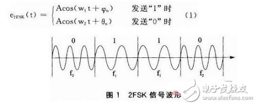
To perform wireless communication, the signal must be modulated. There are many ways to digitally modulate, such as ASK, FSK, PSK, etc. After comprehensive consideration, choose 2FSK modulation which has certain anti-interference ability and is simple and easy to implement. 2FSK uses sine waves of different frequencies to represent digital signals "0" and "1". The frequency of the carrier varies with the binary baseband signal between the two frequencies f1 and f2. The expression is as shown in equation (1), and the 2FSK signal waveform is shown in Fig. 1.
1.2 Electromagnetic induction theory
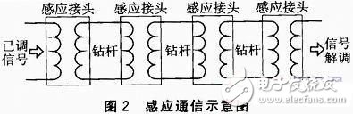
The wireless communication here is actually an inductive communication. Two coils are placed adjacent to the two drill rods, and a change in current in one coil (main coil) generates an alternating magnetic field around it. The magnetic field causes the other coil (secondary coil) to generate an induced electromotive force, which is the principle of inductive communication. The schematic diagram is shown in Figure 2.
2 system hardware design
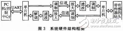
The hardware structure of the system is shown in Figure 3. The whole system takes two single-chip microcomputers as the core, XR2206 and XR2211 as the modulation and demodulation chip, MAX275 as the band-pass filter chip, and the amplification circuit adopts the basic common-emitter amplification circuit. The system can realize two-way communication (not full duplex, only work in half-duplex mode, that is, the channel can be time-multiplexed), the ground mainly transmits control signals downwards, and transmits information such as temperature and pressure downhole, with symmetry above and below. Structure, so only the module for unidirectional signal transmission can be analyzed in the later analysis. Of course, in actual drilling operations, some wells are up to several kilometers deep and require multiple stages of drill pipe cascading. Therefore, after every 3 to 5 stages of drill pipe, the signal needs to be demodulated and amplified, which actually requires a relay module. The relay module performs the functions of demodulation amplification and remodulation.
2.1 Modulation module and demodulation module design
Through the test of the channel characteristics, it is found that when the four-stage drill pipe cascade (40m in total) and the number of turns of the coupled coil are 400åŒ (the copper wire radius of the coupled coil is 0.2mm), when a 120 kHz sine wave is input. The amplitude of the output signal is the largest, indicating that the resonant frequency of the channel formed by the induction coil is 120 kHz, and the carrier frequency can be selected around 120 kHz. Therefore, the XR2206, which is inexpensive and meets the requirements, is used as the modulation chip, and the XR2211 matched with it is used as the demodulation chip. .
XR2206 main performance parameters:
â—†Single-chip integrated function generator, can generate high stability, high precision sine wave, square wave, triangle wave and other waveforms.
â—† The operating frequency ranges from 0.01 Hz to 1 MHz.
◆The working voltage is 10~26 V, and the frequency temperature stability is 20&TImes; 10-6/°C.
The modulation module circuit composed of XR2206 is shown in Fig. 4.
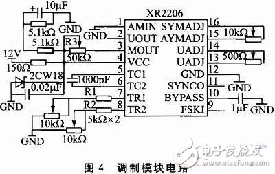
According to the previous analysis, the two carriers selecting 2FSK are f1=110 kHz and f2=130 kHz, respectively, and “1†is modulated on f1, and “0†is modulated on f2. The capacitance between pins 5 and 6 of the XR2206 is the timing capacitor, which is taken as 1000pF. To get f1 and f2, find two timing resistors R1=1/f1c=9.09 kHz, R2=1/f2c=7.7 kHz, where R1 and R2 respectively select a 5 kΩ resistor and then connect a 10 kΩ potentiometer. In order to facilitate accurate adjustment. The digital signal is input from pin 9 and the modulated signal is output from pin 2; the 500 Ω potentiometer connected in series with pins 13 and 14 can improve the output waveform; the potentiometer R3 connected to pin 3 is used to adjust the amplitude of the output; A 16 kΩ potentiometer with 16 pins can improve the distortion of the output sinusoidal waveform.
XR2211 performance parameters:
â—† Operating frequency range is from 0.01 Hz to 300 kHz.
◆ Operating voltage is 4.5 ~ 20 V, frequency temperature stability is 20 & TImes; 10-6 / ° C, HCMOS / TTL / logic compatibility.
â—† Wide dynamic range from 10 mV to 3 Vrms.
The demodulation module circuit composed of XR2211 is shown in FIG. 5.
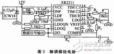
According to the XR2211 chip manual, the relevant parameters are calculated according to their steps. The center frequency, the recommended range of R0 is 10~100 kΩ, where R0=16.67 kΩ is selected, then C0=1/f0R0=500 pF, R1=2R0·f0/(f2-f1)=200 kΩ, C1=1 250&TImes; C0/R10.52=12 pF; Rf≥5R1, take Rf=1 MΩ, RB≥5Rf, take RB=5 MΩ, Rsum=(Rf+R1)RB/(Rf+R1+RB)=967 kΩ; Cf =0.25/(Rsum&TImes; baud rate), when the baud rate is 9 600 b/s, Cf = 27 pF. When the baud rate is other values, the value of Cf can be changed accordingly. If the value calculated above is not a nominal value of resistance or capacitance, the required resistance or capacitance can be formed in series or in parallel.
2.2 Filter circuit design
Due to the harsh channel environment, there are various kinds of noise, and the signals are all drowned in the noise, so the signal needs to be filtered. A bandpass filter is needed here. If an ordinary active filter is selected, the implementation is simple but the parameter adjustment is difficult, and it is used in a high frequency. Since the distributed capacitance around the component will seriously affect the characteristics of the filter, its stability is also poor. Here, the analog integrated active filter MAX275 is selected. The MAX275 can avoid the disadvantages of the active filter. The main characteristic parameters are as follows:
â—† Butterworth, Chebyshev, Bezier type low-pass, band-pass filter can be realized by externally connecting different resistors.
â—† The center frequency of the filter ranges from 0.01 Hz to 300 kHz.
â—† Gain bandwidth product is 16 MHz.
◆ Single 5 V power supply or ±5 V power supply.
The bandpass filter circuit composed of MAX275 is shown in Figure 6.
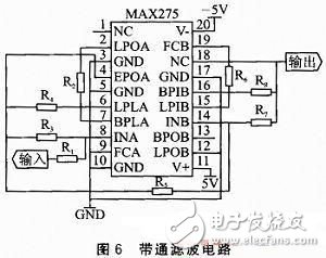
According to the MAX275 manual, the parameters of the peripheral components can be obtained. Since the selected carrier frequencies are 110 kHz and 1 30 kHz, respectively, the center frequency of the bandpass filter is set to 120 kHz, and the two carrier frequencies must be within the passband of the filter. . The passband can be set to 105~135kHz. According to these requirements, the relevant parameters can be obtained: R1=5.1 kΩ, R2=16.7 kΩ (can be realized by 10 kΩ resistor series 10 kΩ potentiometer), R3=16.7 kΩ (can be 10 kΩ resistor in series with a 10 kΩ potentiometer), R4 = 11.7 kΩ (achievable by a 1 kΩ potentiometer with an 11 kΩ resistor in series). Since the MAX275 is a two-stage cascaded filter, the parameters of the two stages can be chosen to be the same, ie R5=R1, R6=R2, R7=R3, R8=R4. The performance of the filter is tested when the circuit is debugged. After obtaining the data, it is drawn by MATLAB, and its amplitude response is shown in Fig. 7.

It can be seen from Fig. 7 that the filter passband range is about 110 to 133 kHz, and the center frequency is about 121 kHz, which can meet the actual requirements.
2.3 Amplifier circuit design
Any communication system is not open to large circuits, and the system is no exception. After the signal passes through the 4-level drill pipe, it is only about 30 mV, which is completely submerged by noise. Therefore, at least the signal should be amplified by more than 100 times to meet the processing requirements of the latter circuit. Amplifier circuits are implemented in many ways, either by discrete components or by integrated op amps. However, it must be noted here that the integrated op amp has a gain-bandwidth product. For example, an op amp with a gain-bandwidth product of 1 MHz is not suitable for amplifying signals with a frequency exceeding 100 kHz. Therefore, an amplifying circuit composed of a triode is used in this paper. When designing the amplifier circuit, pay attention to the selection of the triode with high cutoff frequency. Here, select the high frequency small power tube 3DG100. Make sure that the triode has no cutoff distortion and saturation distortion for the amplification of the useful signal. There are many configurations of the amplifier circuit. The emitter amplification circuit. The first-stage amplifying circuit obviously cannot meet the requirements of amplification. After adopting the two-stage amplifying circuit, the requirements can be satisfied. At the same time, the output and input of the common-emitter amplifier circuit are inverted, and the output and input after the second-stage amplification meet the requirements of the same phase. There are a lot of books on the amplifying circuit for reference, so I won't go into details here.
3 system software design
The software in this system is mainly divided into two parts: one is the test software required in the system debugging process, such as generating a square wave signal of a specific frequency to simulate the binary "1" and "0", adding a keyboard circuit to the periphery of the single chip microcomputer. To flexibly select data with different baud rates for testing; second, software that plays a controlling role in the system work process, used to control the direction of information transmission. The software must be written in accordance with the serial communication protocol between the microcontroller and the computer. If the transmission data is encoded, although the reliability of the communication system can be improved and the bit error rate is lowered, the rate of effective data transmission is affected, so the channel is not encoded here.
4 Test methods and results
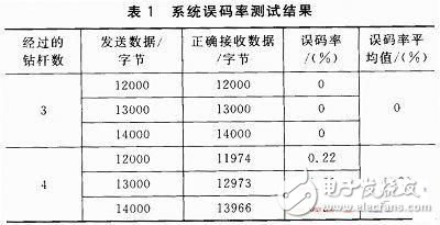
The system's testing follows the principle from part to whole. Each module is tested first, and the entire system is tested after each module is tested. One PC sends data, and the other PC receives data, compares the transmitted data with the received data to get the bit error rate. When the baud rate is 9 600 b/s, the system error rate test results are listed in Table 1.
Conclusion
In this paper, XR2206 and XR2211 are used as the demodulation chip, and AT89C51 is the control chip. A set of FSK inductive communication system is designed and verified in the laboratory, and the baud rate of 9 600 b/s is obtained. The system can be applied to underground operations such as oil and natural gas as well as the detection of marine resources. However, compared with the level of foreign countries, there are still many factors to be considered in the actual application. In terms of device selection, resistors and capacitors with poor precision will affect the quality of the signal, and carrier frequency offset will occur. The impedance matching of the circuit is the biggest problem of the system. The signal is often transmitted under mismatch conditions. The loss of the signal at the coupled coil is quite serious. In addition, the communication rate of the system is not very high due to the limitation of Shannon's theorem. It can be considered to modulate the signal to a higher frequency band, but at this time, it is necessary to add a capacitor, an inductor and the like at the coupling coil to change the resonance point of the channel to make it resonate in a higher frequency band. These problems above need to be carefully studied in future work.
ZGAR Aurora 500 Puffs
ZGAR electronic cigarette uses high-tech R&D, food grade disposable pod device and high-quality raw material. All package designs are Original IP. Our designer team is from Hong Kong. We have very high requirements for product quality, flavors taste and packaging design. The E-liquid is imported, materials are food grade, and assembly plant is medical-grade dust-free workshops.
Our products include disposable e-cigarettes, rechargeable e-cigarettes, rechargreable disposable vape pen, and various of flavors of cigarette cartridges. From 600puffs to 5000puffs, ZGAR bar Disposable offer high-tech R&D, E-cigarette improves battery capacity, We offer various of flavors and support customization. And printing designs can be customized. We have our own professional team and competitive quotations for any OEM or ODM works.
We supply OEM rechargeable disposable vape pen,OEM disposable electronic cigarette,ODM disposable vape pen,ODM disposable electronic cigarette,OEM/ODM vape pen e-cigarette,OEM/ODM atomizer device.

Aurora 500 Puffs,Pod System Vape,Pos Systems Touch Screen,Empty Disposable Vape Pod System,500Puffs Pod Vape System
ZGAR INTERNATIONAL(HK)CO., LIMITED , https://www.zgarette.com