In the semiconductor chip manufacturing equipment, the largest investment and the most critical is the lithography machine. The lithography machine is also a system engineering equipment with the highest accuracy and difficulty, the most intensive technology and the fastest progress. Compared with other lithography technologies, optical lithography has the advantages of high productivity, low cost, high alignment and overlay accuracy, relatively simple mask fabrication, and easy access to process conditions. It has always been a semiconductor chip manufacturing industry. The mainstream lithography technology. Currently, the main lithography equipment in the international semiconductor chip manufacturing line is a 248 nm (KrF) excimer laser projection lithography machine, and is currently transitioning to a 193 nm (ArF) excimer laser projection lithography machine. As one of the world's three largest integrated lithography machine manufacturers, the Dutch ASML Company has been tirelessly carrying out technological innovation to enhance its competitiveness and has been a leader in the global lithography machine sales market.
Asml lithography machine working principle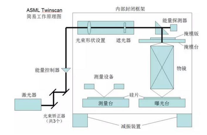
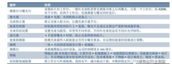
The figure above is an introduction to the ASML lithography machine. Below, briefly introduce the role of each device in the figure.
Measuring table, exposure table: It is a worktable that carries silicon wafers.
Laser: It is the light source, one of the core equipment of the lithography machine.
Beam Corrector: Correct the incident direction of the beam and make the beam as parallel as possible.
Energy Controller: Controls the energy that will eventually shine on the silicon wafer. Underexposed or overexposed will seriously affect the imaging quality.
Beam shape setting: Set the beam to round, ring and other shapes, different beam states have different optical characteristics.
Shutter: Blocks the beam from shining on the wafer when exposure is not needed.
Energy detector: Detects whether the final incident energy of the beam meets the exposure requirements and feeds it back to the energy controller for adjustment.
A mask plate: A glass plate engraved with a circuit diagram on the inside, costing hundreds of thousands of dollars.
Masking station: The equipment that carries the motion of the mask, the motion control accuracy is nm level.
Objective: The objective lens is used to compensate for optical errors, and the circuit diagram is scaled down.
Wafer: A wafer made of silicon crystal. There are many sizes of silicon wafers, and the larger the size, the higher the yield. Digression, because the silicon is round, so need to cut a gap in the silicon wafer to confirm the wafer's coordinate system, according to the shape of the gap is divided into two different, respectively called flat, notch.
Internal closed frame and shock absorber: isolate the work table from the external environment, maintain the level, reduce the external vibration interference, and maintain a stable temperature and pressure.
In the processing of the chip, the lithography machine transmits a beam of light through a series of light source energy and shape control means through a mask drawing a circuit diagram, compensates for various optical errors through the objective lens, and maps the line picture after being scaled down to Silicon wafers are then chemically developed to obtain a circuit diagram carved on the silicon wafer. The general lithography process is subject to processes such as cleaning, drying, coating, spin coating, soft bake, alignment exposure, post-baking, developing, hard-baking, and laser etching. After a photolithography chip can continue to glue, exposure. The more complex the chip, the more layers of the circuit diagram, also need a more sophisticated exposure control process.
The three most important technical indicators of the excimer laser scanning stepper lithography machine are: lithography resolution, Overlay accuracy, and Production2tivity.
The lithography resolution formula is:
CD=K1・λ/NA
Where λ is the excimer laser output laser wavelength, K1 is the process factor factor, and NA is the projection lithography objective lens numerical aperture. It can be seen from the above equation that increasing the lithographic resolution can be achieved by shortening the laser wavelength, reducing the process factor factor K1, and increasing the numerical aperture NA of the projection lithography objective lens. Shortening the laser wavelength will involve a series of technical issues such as lasers, optical system design, optical materials, optical coatings, optical path contamination, and exposure resists; low process factor K1 value imaging, only when mask design, lighting conditions, and resists Process optimization can only be achieved at the same time. For this purpose, it is necessary to use off-axis illumination, phase shift masking, optical proximity correction, pupil filtering and other technical measures; the numerical aperture of the projection lithography lens and the laser wavelength and spectral bandwidth. , imaging field of view, optical design and optical processing level and other factors.
Engraving accuracy is closely related to lithography resolution. If the 0.10 μm lithographic resolution is to be achieved, the overlay accuracy must not be less than 0.03 μm according to the 33% rule. The overlay accuracy is mainly related to the positioning accuracy of the workpiece stage and the mask stage, the optical alignment accuracy, the synchronization scan accuracy, and the positioning accuracy, the alignment accuracy, and the synchronization scan accuracy are about 1/5 to 1/3 of the overlay accuracy, respectively. , ie 0.006 to 0.01 μm. Enhancing production efficiency is a necessary condition for industrialization of photolithography machines. In order to improve production efficiency, it is necessary to optimize the design of laser output power, repetition frequency, exposure energy control, synchronous scanning, and other technical links, and adopt advanced technologies to minimize the time required for the steps of changing the film, stepping, and optical alignment.
The light source of the lithography machine is the core, and EUV is the cutting edge of next-generation lithography. The light source used by the lithography machine has several requirements:
There are suitable wavelengths (the shorter the wavelength, the smaller the feature size of the exposure), at the same time there is enough energy, and it is evenly distributed in the exposed area.
A direct way to achieve photolithographic advancement is to reduce the wavelength of the light source used. The early UV source was a high-pressure arc lamp (high-pressure mercury lamp), which was filtered using g-line (436 nm) or i-line (365 nm). A deeper UV light source with a shorter wavelength is an excimer laser that uses electron beams to excite gas molecules formed by the combination of an inert gas and a halogen gas, and generates a laser when it transitions to the ground state, which is characterized by directionality. Strong, high wavelength purity, high output power, such as KrF (248 nm), ArF (193 nm) and F2 (157 nm). The dry lithography machine with 193nm ArF light source has a lithography process node of 45nm. After the immersion and optical proximity correction techniques are used, the limit lithography process node can reach 28nm.
Key components of mainstream lithography machines
The first dual workbench significantly increased production efficiency. Before lithography equipment 2000, there was only one workbench where wafer alignment and etching processes were completed. The Twinscan dual stage system introduced by the company in 2001 is a major advancement in the industry, enabling the lithography machine to expose the wafers on one worktable while performing pre-alignment work on another workbench, and for the first time. With feedback from the results, production efficiency increased by approximately 35% and accuracy increased by more than 10%. Although the two-workpiece table system only adds one work table, the technical difficulty is not to be underestimated, and there is a very high requirement for the worktable transfer speed and accuracy. Asmar's exclusive magnetically suspended workpiece table system enables the system to overcome the friction coefficient and damping coefficient, and its machining speed and precision exceed the mechanical and air floatation workpiece table.

Dual-table lithography apparatus construction diagram
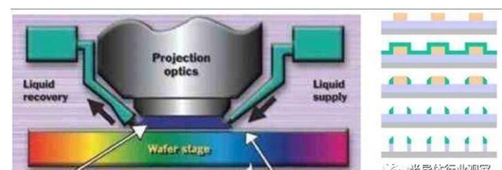
Immersion lithography and secondary exposure enhance process capabilities to fill the evolution gap before the advent of EUV. Immersion lithography is the addition of a special layer of water or liquid between the lens and the silicon wafer. Light is immersed in the liquid and exposed on the silicon wafer circle. Because the refractive index of the liquid is higher than that of air, the imaging accuracy is higher. . Get better resolution and smaller exposure size.
In 2002, the industry proposed 193nm immersion lithography equipment planning, because the refractive index of 193nm spectrum in water up to 1.44 (the higher the refractive index, the better the etching accuracy), the equivalent wavelength is shortened to 134nm, equipment manufacturers only need to With minor modifications to existing equipment, the accuracy of etching can be increased by 1-2 generations. Asimia first introduced the 193nm immersive device, the effect is better than the 157nm light source equipment, successfully upgraded the 90nm process to 65nm, and completely defeated the Nikon and Canon line of the dry etching route, which is an important turning point in the industry structure.
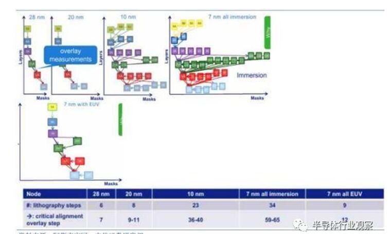
After 2010, the process technology has evolved to 22nm, which has surpassed the etching accuracy of the immersed DUV, so the industry began to introduce two pattern exposure processes to produce lines in an indirect way; that is, not directly exposing the pipeline section but exposing it first. Both sides of the wall, indirectly forming the line area. Although the double exposure can produce an integrated circuit with a higher accuracy than the light source, the side effect is that the number of photolithography and the number of masks are greatly increased, resulting in increased costs and prolonged production cycles. Therefore, the light source with shorter wavelength and higher precision is only improved. The key to process capability. For ArF lithography using immersion + double pattern exposure, the process node limit is 10 nm. The EUV lithography machine is expected to extend the process to 7nm and 5nm.
Immersion lithography and secondary pattern exposure
The biggest bottleneck in the semiconductor industry is that the cost of realizing Moore's Law is increasing, and the process miniaturization is no longer accompanied by a simultaneous drop in transistor unit costs. When moving from the 32/28nm node to the 22/20nm node, due to the lack of lithographic precision, it is necessary to use technologies such as double exposure to realize the increase in equipment and manufacturing costs, and the unit cost of the transistor will rise for the first time.
The industry is pinning its hopes on extreme ultraviolet (EUV) lithography technology, expecting the high precision of EUV equipment, helping manufacturers to reduce the number of lithography processes and increasing wafer production volume below 7nm. In 2013, Asimia’s EUV lithography equipment was successfully developed. The wavelength of the light source is 22nm, and the technology is gradually advancing. In 2017, the device has adopted the minimum 13nm EUV as the light source, and the ultra-short wavelength enables the feature size exposure below 7nm to be realized. As the industry process goes below 10nm, a more advanced EUV lithography system is needed, and only Asimah's NXE series can meet the demand.
Advanced Process Complexity and EUV Equipment Benefits
The EUV process brings together top technologies in many fields. EUV must be mass-produced, and several technical bottlenecks must be overcome; first on the light source. The EUV has a wavelength of 13.5 nm. This light is easily absorbed by the material contained in the lens glass. Therefore, a mirror is used instead of a lens. The reflectance of an ordinary polished mirror is not high enough and a Bragg reflector must be used. A dual-mirror design that concentrates multiple layers of reflection into a single reflection.
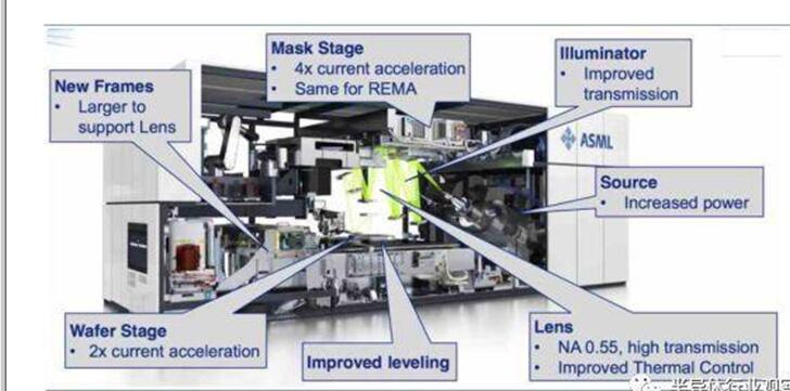
In addition, the gas absorbs EUV and affects the refractive index, so vacuum must be used in the chamber. In order to solve the problem of light source of EUV, in October 2012, Asmy spent EUR1.95 billion to acquire Cymer, its key optical technology provider, to accelerate the development of EUV related technologies. The company's 2017 EUV device, the NXE 3400B, has successfully increased the light source power and accuracy, achieved a line width of approximately 13 nanometers, and used a magnetic levitation system to accelerate masks and worktables. It is expected that the throughput will be as high as 125 wafers per hour. The tolerances for overlays are within 3 nanometers.
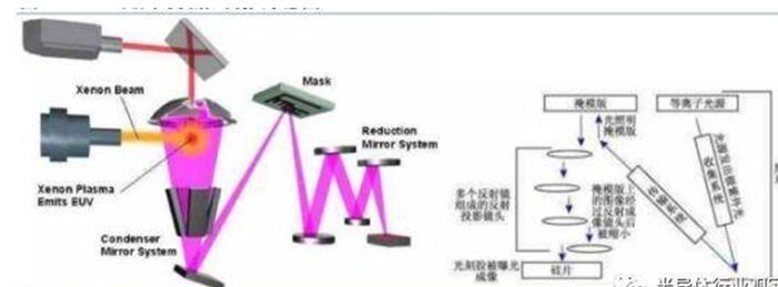
EUV lithography and reflective lens diagram
In the past DUV period, a 7nm process that required multiple masks was required. The new EUV system is expected to be completed with a single mask step; however, at a process of 5nm or less, multiple image exposure problems will still be encountered. Improve the capabilities of next-generation EUV devices beyond the light source. To this end, the company acquired a 24.9% stake in Carl Zeiss, an optical giant, for $1.1 billion in 2016 and promised $840 million in R&D investment to jointly develop a lens with a numerical aperture (NA) higher than 0.5. The second-generation EUV lithography is expected to be in volume production after 2024, when it is planned to achieve a line width of about 8 nanometers, processing 185 wafers per hour, and the tolerance of tolerances is less than 2 nanometers.
Asmar's generous investment in ZEISS for joint development shows Asimia's determination to succeed in the next generation of EUV equipment. The process of importing EUVs by giants is different, and equipment requirements can last for more than three years. After entering the 7nm process generation, the global semiconductor industry is expected to be the top three duel between Taiwan Semiconductor Manufacturing Co., Samsung Electronics, and the Global Alliance. In 2012, Samsung and TSMC respectively injected capital of 500 million and 1.5 billion euros to Asmar in order to strengthen their strategic cooperation with the company;
According to the various roadmaps compiled by the research organization Anandtech, TSMC is the fastest to reach 7nm process manufacturers. Taiwan Semiconductor Manufacturing Co., Ltd. announced that it is tailor-made for the high-speed computing market and tailored its platform for artificial intelligence and data analysis. It is estimated that H1 will have 7nm mass production capacity in 2018, followed by the second generation of 7nm in 2019, and introduction of Asim's EUV. Equipment, and is expected to test production of 5nm process products in the same year. In terms of other manufacturers, Samsung decided to make EUV technology available directly at the 7nm generation of the first generation in 2018, and Groffield inherited IBM's own research and development of 7nm. It is also expected to mass production in the second half of 2018, but the first generation is to use it. DUV, and the introduction of EUV takes 2019. Intel, due to cost considerations, will not begin to replace the 10nm process with 7nm process until 2021.
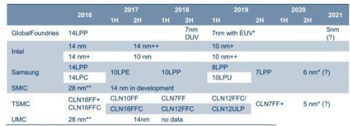
Advanced process routes from major wafer vendors
Focus on the advantages of photolithography to expand technology and create rigid customer needs
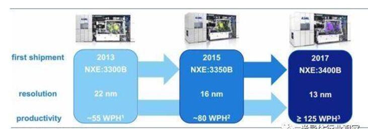
The company has obvious technological advantages and maintains its leading position in the industry. In 2013, the company first introduced the EUV device NXE 3300B.
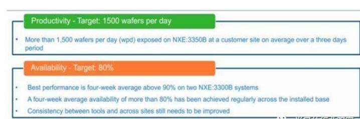
However, the accuracy and efficiency do not have the production efficiency below 10nm; until the 3400B after 2016, the optical and electromechanical system technology breakthrough, the wavelength of the EUV light source was shortened to 13nm, 125 wafers per hour were processed, or daily 1500 tablets; the average production yield for 4 weeks is 80%, with high productivity and high precision. As the chip size continues to shrink, EUV equipment has not yet become an industry need. At present, the world's first-line logic wafers and memory wafer vendors are purchasing Asimian TWINSCAN models, among which Intel, Samsung, and TSMC's three giants have all staked in Aspen. Mak, in order to seek the co-development of its high-end lithography equipment and priority procurement rights.
EUV lithography machine NXE3400B construction schematic
Thanks to the company's immersive EUV lithography equipment, customers can implement mass-produced wafer processes of 7nm and 5nm, and achieve 2.5nm accuracy, and the shipment volume will be considerable in the future. In the first half of 2017, the company sold 2 EUV equipment, and Q3 doubled to 4 units in a single quarter. It is expected that there will be 6 units delivered in Q4, which will bring 300 million euros of single-quarter revenue. It plans to sell more than 20 units in 2018 and 19 years.
Asmar EUV lithography equipment TWINSCAN NXE series
Overall, the company achieved revenue of 1.8 billion euros in the 2017Q3 quarter, with the top three product lines being ArF (63%), EUV (21%) and KrF (10%). The demand for KrF dry lithography systems from 3D NAND customers continues to increase. Currently, over 20 non-shipping orders have been accumulated for related equipment, showing that the company's mid- to high-end products all occupy market leadership positions.
In modern clinical medicine, ventilator, as an effective means to artificially replace the function of spontaneous ventilation, has been widely used in respiratory failure caused by various reasons, anesthesia and respiratory management during major surgery, respiratory support treatment and emergency resuscitation. It occupies a very important position in the field of modern medicine. A ventilator is a vital medical device that can prevent and treat respiratory failure, reduce complications, and save and prolong patients' lives.
With excellent quality and preferential prices, Kable-X (Su Zhou) Technology Co., Ltd. provides services for the wiring harness industry in various fields such as industrial control, medical care, automobiles, and new energy. It has obtained IATF16949\ISO9001\ISO14000\UL\ISO13485\IPC620, etc. Industry certification. At the same time, the company also passed the certification of high-tech enterprises in 2019 and obtained a number of industry patents. It has the ability to integrate wiring harnesses and electronic components and hardware injection molding parts. It actively participates in customers' initial product design selection, and Maintain the greatest flexibility to meet the various needs of customers. Punctual delivery to meet customer needs. Suzhou Kable-X Wire Harness Processing Factory adheres to the business philosophy of "Integrity, Responsibility, Innovation", and perfect after-sales service to create together with customers. A better tomorrow!"
We produce a large number of Medical Cable Assembly, including Ventilator Wire Harness, Medical Defibrillator Wire Harness and Medical Aid Equipment Wire Harness.

Ventilator Wire Harness,Wire Harness Manufacturing,Wiring Harness Price,Electronic Wiring Harness Assembly
Kable-X Technology (Suzhou) Co., Ltd , https://www.kable-x-tech.com