IGBT (Insulated Gate Bipolar Transistor), insulated gate bipolar transistor, is a composite fully controlled voltage-driven power composed of BJT (bipolar transistor) and MOS (insulated gate field effect transistor). The semiconductor device combines the advantages of both the high input impedance of the MOSFET and the low on-voltage drop of the GTR. The GTR saturation voltage is reduced, the current carrying density is large, but the driving current is large; the MOSFET driving power is small, the switching speed is fast, but the conduction voltage drop is large, and the current carrying density is small. The IGBT combines the advantages of the above two devices, with low driving power and reduced saturation voltage. It is very suitable for converter systems with DC voltages of 600V and above, such as AC motors, inverters, switching power supplies, lighting circuits, traction drives, etc.
structure
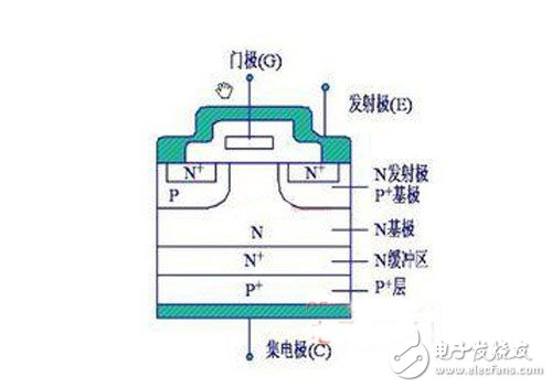
The left side of the IGBT structure diagram shows an N-channel enhancement type insulated gate bipolar transistor structure. The N+ region is called the source region, and the electrode attached to it is called the source. The P+ zone is called the drain zone. The control region of the device is the gate region, and the electrode attached thereto is called the gate. The channel is formed next to the boundary of the gate region. The P-type region (including the P+ and P-regions) between the drain and the source (the channel is formed in this region) is called a Subchannel region. The P+ region on the other side of the drain region is called a drain injector. It is a unique functional region of the IGBT. Together with the drain region and the sub-channel region, a PNP bipolar transistor is formed to function as an emitter. The drain injects holes and conducts conductive modulation to lower the on-state voltage of the device. The electrode attached to the drain implant region is called the drain.
The switching function of the IGBT is to form a channel by adding a forward gate voltage, and provide a base current to the PNP (formerly NPN) transistor to turn on the IGBT. Conversely, the reverse gate voltage is applied to eliminate the channel, and the base current is cut off to turn off the IGBT. The driving method of the IGBT is basically the same as that of the MOSFET, and it only needs to control the input pole N-channel MOSFET, so it has high input impedance characteristics. When the channel of the MOSFET is formed, the hole from the P+ base is injected into the N-layer (small sub-), and the N-layer is conductance modulated to reduce the resistance of the N-layer, so that the IGBT also has a low voltage at a high voltage. On-state voltage.
Working characteristics
The static characteristics of IGBTs mainly include volt-ampere characteristics, transfer characteristics and switching characteristics.
The volt-ampere characteristic of the IGBT is the relationship between the drain current and the gate voltage when the gate-source voltage Ugs is used as a parameter. The output drain current is controlled by the gate-source voltage Ugs. The higher the Ugs, the larger Id. It is similar to the output characteristics of the GTR. It can also be divided into a saturated zone 1, an enlarged zone 2, and a breakdown characteristic 3 part. In the off-state IGBT, the forward voltage is taken over by the J2 junction and the reverse voltage is taken up by the J1 junction. If there is no N+ buffer, the forward and reverse blocking voltage can be achieved at the same level. After the N+ buffer is added, the reverse shutdown voltage can only reach tens of volts, thus limiting the application range of the IGBT.
The transfer characteristic of the IGBT is a relationship between the output drain current Id and the gate-source voltage Ugs. It has the same transfer characteristics as the MOSFET. When the gate-source voltage is less than the turn-on voltage Ugs(th), the IGBT is turned off. Id is linear with Ugs over most of the drain current range after the IGBT is turned on. The maximum gate-to-source voltage is limited by the maximum drain current, and the optimum value is generally about 15V.
The switching characteristics of the IGBT refer to the relationship between the drain current and the drain-source voltage. When the IGBT is in the on state, its PNP transistor is a wide base transistor, so its B value is extremely low. Although the equivalent circuit is a Darlington structure, the current flowing through the MOSFET becomes a major part of the total current of the IGBT. At this time, the on-state voltage Uds(on) can be expressed by
Uds(on) = Uj1 + Udr + IdRoh
Where Uj1 is the forward voltage of the JI junction, which is 0.7 to 1V; Udr is the voltage drop across the extended resistor Rdr; Roh is the channel resistance.
The on-state current Ids can be expressed by:
Ids=(1+Bpnp)Imos
Where Imos is the current flowing through the MOSFET.
Due to the conductance modulation effect in the N+ region, the on-state voltage drop of the IGBT is small, and the on-state voltage drop of the IGBT with a withstand voltage of 1000V is 2 to 3V. When the IGBT is in the off state, only a small leakage current exists.
Dynamic characteristics
During the turn-on process, the IGBT is operated as a MOSFET most of the time, except that after the drain-source voltage Uds falls, the PNP transistor is amplified from the amplification region to a delay time. Td(on) is the turn-on delay time and tri is the current rise time. The drain current turn-on time ton, which is often given in practical applications, is the sum of td (on) tri . The falling time of the drain-source voltage consists of tfe1 and tfe2.
The triggering and turn-off of the IGBT requires a forward voltage and a negative voltage between the gate and the base. The gate voltage can be generated by different drive circuits. When selecting these driver circuits, they must be based on the following parameters: device turn-off bias requirements, gate charge requirements, solidity requirements, and power conditions. Because the IGBT gate-emitter impedance is large, MOSFET drive technology can be used for triggering. However, since the input capacitance of the IGBT is larger than that of the MOSFET, the turn-off bias of the IGBT should be better than many MOSFETs.
During the turn-off of the IGBT, the waveform of the drain current becomes two segments. Since the stored charge of the PNP transistor is difficult to be quickly removed after the MOSFET is turned off, the tail current of the drain current is long, td(off) is the turn-off delay time, and trv is the rise time of the voltage Uds(f). The drop time Tf of the drain current often given in practical applications is composed of two segments t(f1) and t(f2) in the figure, and the off time of the drain current.
t(off)=td(off)+trv ten t(f)
In the formula, the sum of td(off) and trv is also called storage time.
The switching speed of the IGBT is lower than that of the MOSFET, but it is significantly higher than the GTR. The IGBT does not require a negative gate voltage to turn off the turn-off time when turned off, but the turn-off time increases as the gate and emitter shunt resistance increases. The turn-on voltage of the IGBT is about 3 to 4V, which is equivalent to the MOSFET. The saturation voltage drop when the IGBT is turned on is lower than that of the MOSFET and is close to the GTR, and the saturation voltage drop decreases as the gate voltage increases.
The voltage and current capacity of the officially commercial IGBT devices are still very limited, far from meeting the needs of the development of power electronics application technology; in many applications in the high voltage field, the voltage level of the device is required to reach 10KV or more, and currently only through the IGBT high voltage series connection, etc. Technology to achieve high pressure applications. Some foreign manufacturers, such as Swiss ABB, have developed 8KV IGBT devices using the soft-through principle. The 6500V/600A high-voltage and high-power IGBT devices produced by Germany's EUPEC have been put into practical use. Toshiba has also been involved in this field. At the same time, major semiconductor manufacturers continue to develop high voltage, high current, high speed, low saturation voltage drop, high reliability, low cost technology of IGBT, mainly using the production process below 1um, and some new progress has been made in research and development.
Communication Ladder Backup Lithium Battery System
51.2V Lithium Battery System,Bms Function Battery System,High Energy Density Battery,Custom Lithium Battery System
Wolong Electric Group Zhejiang Dengta Power Source Co.,Ltd , https://www.wldtbattery.com